npj 2D Materials and Applications ( IF 9.1 ) Pub Date : 2019-12-04 , DOI: 10.1038/s41699-019-0130-6 Francisco Pasadas , Enrique G. Marin , Alejandro Toral-Lopez , Francisco G. Ruiz , Andrés Godoy , Saungeun Park , Deji Akinwande , David Jiménez
|
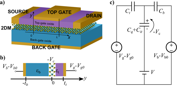
We present a physics-based circuit-compatible model for double-gated two-dimensional semiconductor-based field-effect transistors, which provides explicit expressions for the drain current, terminal charges, and intrinsic capacitances. The drain current model is based on the drift-diffusion mechanism for the carrier transport and considers Fermi–Dirac statistics coupled with an appropriate field-effect approach. The terminal charge and intrinsic capacitance models are calculated adopting a Ward–Dutton linear charge partition scheme that guarantees charge conservation. It has been implemented in Verilog-A to make it compatible with standard circuit simulators. In order to benchmark the proposed modeling framework we also present experimental DC and high-frequency measurements of a purposely fabricated monolayer MoS2-FET showing excellent agreement between the model and the experiment and thus demonstrating the capabilities of the combined approach to predict the performance of 2DFETs.
中文翻译:
2DFET的大信号模型:终端电荷和本征电容的紧凑模型
我们提出了基于栅极的二维基于半导体的场效应晶体管的基于物理的电路兼容模型,该模型为漏极电流,端电荷和本征电容提供了明确的表达式。漏极电流模型基于载流子迁移的漂移扩散机制,并考虑了费米-狄拉克统计量以及适当的场效应方法。终端电荷和本征电容模型采用Ward-Dutton线性电荷分配方案进行计算,以保证电荷守恒。它已在Verilog-A中实现,以使其与标准电路模拟器兼容。为了对建议的建模框架进行基准测试,我们还介绍了故意制造的单层MoS 2的实验性直流和高频测量-FET在模型与实验之间显示出极好的一致性,从而证明了组合方法可预测2DFET的性能。


 京公网安备 11010802027423号