Electronic Materials Letters ( IF 2.1 ) Pub Date : 2020-10-21 , DOI: 10.1007/s13391-020-00253-w Yeqing Sun , Ziyang Zhang , Kyeiwaa Asare-Yeboah , Sheng Bi , Zhengran He
|
Abstract
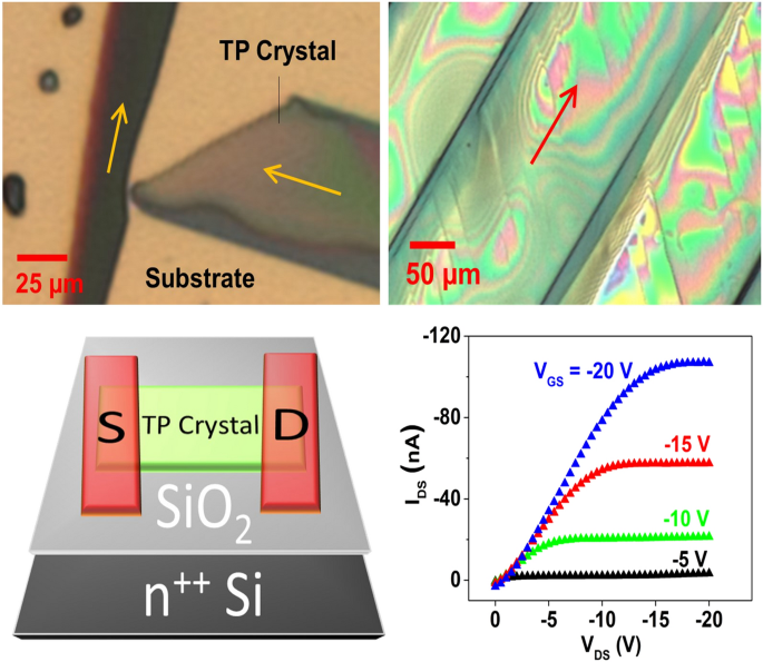
Despite solution processed organic semiconductors have attracted much research attention, the randomized crystallization and large prevalence of grain boundary remain as a challenge to realize high performance organic electronic applications. In this work, we report the incorporation of poly(butyl acrylate) polymer additive with organic semiconductors with the mediation of a solvent vapor annealing method in order to modify the nucleation and crystal growth process. As 6,13-bis(triisopropylsilylethynyl) pentacene (TIPS pentacene) was experimented as a benchmark semiconductor, we demonstrated that the TIPS pentacene/poly(butyl acrylate) mixture exhibits rigidly aligned crystals, large grain width and improved areal coverage. In particular, thin film morphological characterization indicated a substantial reduction in misorientation angle by approximately two orders of magnitude as well as a 5-fold enlargement of grain width. A grain boundary model is proposed as a theoretic basis to understand the connection between grain width and hole mobility. Bottom-gate, top-contact thin film transistors based on TIPS pentacene/poly(butyl acrylate) blends demonstrated enhanced hole mobility of up to 0.11 cm2/Vs.
Graphic Abstract
中文翻译:
溶液加工有机薄膜晶体管用聚丙烯酸丁酯聚合物制成的大尺寸有机半导体晶体
摘要
尽管溶液处理的有机半导体引起了很多研究关注,但是随机晶化和晶界的普遍存在仍然是实现高性能有机电子应用的挑战。在这项工作中,我们报告了在溶剂蒸汽退火方法的介导下,将聚丙烯酸丁酯聚合物添加剂与有机半导体结合在一起,以改变成核和晶体生长过程。以6,13-双(三异丙基甲硅烷基乙炔基)并五苯(TIPS并五苯)作为基准半导体进行了实验,我们证明了TIPS并五苯/聚丙烯酸丁酯混合物显示出刚性排列的晶体,较大的晶粒宽度和改善的面覆盖率。尤其是,薄膜的形态学表征表明,取向错误的角度大幅度降低了大约两个数量级,晶粒宽度扩大了5倍。提出了晶界模型作为理论基础,以了解晶粒宽度和空穴迁移率之间的关系。基于TIPS并五苯/聚丙烯酸丁酯混合物的底栅,顶接触薄膜晶体管的空穴迁移率高达0.11 cm2 / Vs。


 京公网安备 11010802027423号