Journal of Solid State Electrochemistry ( IF 2.6 ) Pub Date : 2020-10-06 , DOI: 10.1007/s10008-020-04832-7 M. A. Contreras-Ruiz , A. Mendez-Blas , Ma. Estela Calixto
|
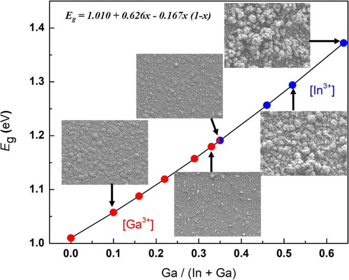
Band gap tuning of electrodeposited Cu(In1-x,Gax)Se2 thin films through varying In3+ and Ga3+ concentrations in the electrolytic bath is demonstrated. Cyclic voltammetry was used to determine best Cu(In1-x,Gax)Se2 deposition potentials at the different bath conditions. Band gap tuning of Cu(In1-x,Gax)Se2 was achieved, through incorporation of varying In3+ and Ga3+ levels during film growth, in the range of 1 to 1.4 eV, corresponding to Ga content 0 ≤ Ga/(In + Ga) ≤ 0.64. Deposited films were characterized by EDS/SEM, XRD, and Raman spectroscopy to determine chemical composition, morphology, and crystal structure. Results show that as-deposited Cu(In1-x,Gax)Se2 thin films are of low crystallinity, with Se and Cu-Se compounds present as a secondary phase. Selenization of electrodeposited Cu(In1-x,Gax)Se2 films was performed using a rapid thermal processing system at 550 °C in an overpressure reactive atmosphere of N2/H2 (96%:4%) and elemental Se vapor. Selenization treatment promoted recrystallization and elimination of secondary phases, resulting in an increase in grain size while maintaining film composition. Processed films with Ga/(In + Ga) = 0.35 were processed into devices, achieving 2.6% efficiency.
中文翻译:
使用快速热退火系统通过电沉积和随后的硒化对Cu(In,Ga)Se 2薄膜进行带隙调谐
通过改变电解槽中In 3+和Ga 3+的浓度,对电沉积Cu(In 1- x,Ga x)Se 2薄膜的带隙调谐进行了说明。循环伏安法用于确定在不同浴条件下的最佳Cu(In 1- x,Ga x)Se 2沉积电位。通过掺入变化的In 3+和Ga 3+实现了Cu(In 1- x,Ga x)Se 2的带隙调谐薄膜生长过程中的水平处于1至1.4 eV的范围内,对应于Ga含量0≤Ga /(In + Ga)≤0.64。通过EDS / SEM,XRD和拉曼光谱对沉积的膜进行表征,以确定化学组成,形态和晶体结构。结果表明,沉积态的Cu(In 1- x,Ga x)Se 2薄膜结晶度低,Se和Cu-Se化合物为第二相。在N 2 / H 2超压反应气氛中,使用快速热处理系统在550°C下进行电沉积的Cu(In 1- x,Ga x)Se 2膜的硒化(96%:4%)和元素硒蒸气。硒化处理促进了再结晶和消除了第二相,从而在保持膜组成的同时增加了晶粒尺寸。Ga /(In + Ga)= 0.35的已处理薄膜被加工成器件,实现了2.6%的效率。


 京公网安备 11010802027423号