Our official English website, www.x-mol.net, welcomes your
feedback! (Note: you will need to create a separate account there.)
Reduction of the ambient effect in multilayer InSe transistors and a strategy toward stable 2D-based optoelectronic applications.
Nanoscale ( IF 5.8 ) Pub Date : 2020-09-01 , DOI: 10.1039/d0nr04120c Yanhao Wang 1 , Jianwei Gao 1 , Bin Wei 2 , Yingkuan Han 2 , Chao Wang 1 , Yakun Gao 1 , Hong Liu 3 , Lin Han 1 , Yu Zhang 1
Nanoscale ( IF 5.8 ) Pub Date : 2020-09-01 , DOI: 10.1039/d0nr04120c Yanhao Wang 1 , Jianwei Gao 1 , Bin Wei 2 , Yingkuan Han 2 , Chao Wang 1 , Yakun Gao 1 , Hong Liu 3 , Lin Han 1 , Yu Zhang 1
Affiliation
|
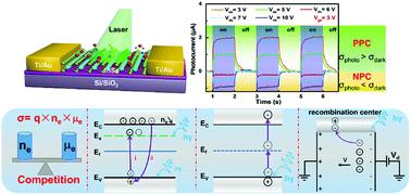
Indium selenide (InSe) photodetection devices attract significant research interest. However, InSe is unstable and degrades rapidly in ambient conditions, thus it is still a challenge to fabricate stable optoelectronic devices. In this work, multilayer InSe FETs are fabricated, and their photoresponse properties are investigated. Both positive and negative photoconductivities are observed for the first time in the same InSe FET in a wide spectral range from 450 nm to 660 nm, which can be tuned through changing either the gate bias or the source–drain bias. A physical mechanism is proposed to explain the dual-photoresponse phenomenon in our devices. Based on the proposed physical mechanism, as a proof of concept, a facile and simple approach is used to eliminate the negative photoconductivity of the InSe FET. Our results will offer valuable strategies for stable multilayer InSe optoelectronic device design, and a practical scheme for improving the performance of other transition metal dichalcogenide devices as well.
中文翻译:

减少多层InSe晶体管中的环境影响,以及实现基于2D的稳定光电应用的策略。
硒化铟(InSe)光检测设备引起了广泛的研究兴趣。但是,InSe不稳定并且在环境条件下会迅速降解,因此制造稳定的光电器件仍然是一个挑战。在这项工作中,制造了多层InSe FET,并研究了它们的光响应特性。在同一InSe FET中,在450 nm至660 nm的宽光谱范围内首次观察到正光电导率和负光电导率,可以通过改变栅极偏置或源极-漏极偏置对其进行调整。提出了一种物理机制来解释我们设备中的双重光响应现象。基于提出的物理机制,作为概念验证,一种简便的方法可用来消除InSe FET的负光电导性。
更新日期:2020-09-18
中文翻译:
减少多层InSe晶体管中的环境影响,以及实现基于2D的稳定光电应用的策略。
硒化铟(InSe)光检测设备引起了广泛的研究兴趣。但是,InSe不稳定并且在环境条件下会迅速降解,因此制造稳定的光电器件仍然是一个挑战。在这项工作中,制造了多层InSe FET,并研究了它们的光响应特性。在同一InSe FET中,在450 nm至660 nm的宽光谱范围内首次观察到正光电导率和负光电导率,可以通过改变栅极偏置或源极-漏极偏置对其进行调整。提出了一种物理机制来解释我们设备中的双重光响应现象。基于提出的物理机制,作为概念验证,一种简便的方法可用来消除InSe FET的负光电导性。


 京公网安备 11010802027423号