当前位置:
X-MOL 学术
›
MRS Commun.
›
论文详情
Our official English website, www.x-mol.net, welcomes your
feedback! (Note: you will need to create a separate account there.)
Electronic structure of technologically important interfaces and heterostructures
MRS Communications ( IF 1.8 ) Pub Date : 2020-12-01 , DOI: 10.1557/mrc.2020.63 Richard Haight
MRS Communications ( IF 1.8 ) Pub Date : 2020-12-01 , DOI: 10.1557/mrc.2020.63 Richard Haight
|
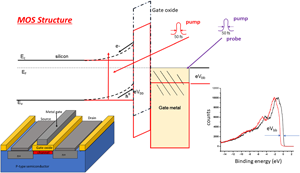
From thin-film solar cells to metal–oxide–semiconductor (MOS) devices in leading-edge integrated circuits, the electronic structure at and near the interfaces between component materials determines the most important fundamental operating characteristics of those devices, such as turn-on voltage, power dissipation, and off-state current leakage. Fermi-level location at buried interfaces, semiconductor (SC) band bending, charge transfer, oxide defects, and work functions of the constituent materials all contribute to device performance. This paper describes how these important parameters can be determined by employing femtosecond photovoltage spectroscopy, an extension of ultraviolet photoelectron spectroscopy (UPS) using ultrafast lasers. While standard UPS is fundamentally a surface-sensitive spectroscopy, pump/probe techniques add a new dimension to this venerable spectroscopy, permitting the accurate extraction of the underlying band bending in SCs. When combined with the valence-band-edge location of the SC and oxide, and determination of the system Fermi level, full characterization of the electronic structure of a MOS stack can be obtained providing key insights on device operating properties. This approach can be extended to study key device materials in emerging areas of artificial intelligence and quantum computing. In each case, surprising new details are uncovered that lead to performance optimization of these technologically important devices. https :// doi.org/10.1557/mrc.2020.63
中文翻译:

技术上重要的界面和异质结构的电子结构
从薄膜太阳能电池到前沿集成电路中的金属氧化物半导体 (MOS) 器件,组件材料之间界面处和附近的电子结构决定了这些器件最重要的基本工作特性,例如导通电压、功耗和断态漏电流。埋入界面处的费米能级位置、半导体 (SC) 带弯曲、电荷转移、氧化物缺陷和组成材料的功函数都有助于器件性能。本文介绍了如何通过使用飞秒光电压光谱法(使用超快激光器的紫外光电子光谱法 (UPS) 的扩展)来确定这些重要参数。虽然标准 UPS 从根本上来说是一种表面敏感的光谱仪,泵/探针技术为这种古老的光谱学增加了一个新的维度,允许准确提取 SCs 中潜在的带弯曲。当结合 SC 和氧化物的价带边缘位置以及系统费米能级的确定时,可以获得 MOS 堆栈的电子结构的完整表征,提供对器件操作特性的关键见解。这种方法可以扩展到研究人工智能和量子计算新兴领域的关键器件材料。在每种情况下,都会发现令人惊讶的新细节,从而优化这些技术上重要的设备的性能。https://doi.org/10.1557/mrc.2020.63 当结合 SC 和氧化物的价带边缘位置以及系统费米能级的确定时,可以获得 MOS 堆栈的电子结构的完整表征,提供对器件操作特性的关键见解。这种方法可以扩展到研究人工智能和量子计算新兴领域的关键器件材料。在每种情况下,都会发现令人惊讶的新细节,从而优化这些技术上重要的设备的性能。https://doi.org/10.1557/mrc.2020.63 当结合 SC 和氧化物的价带边缘位置以及系统费米能级的确定时,可以获得 MOS 堆栈的电子结构的完整表征,提供对器件操作特性的关键见解。这种方法可以扩展到研究人工智能和量子计算新兴领域的关键器件材料。在每种情况下,都会发现令人惊讶的新细节,从而优化这些技术上重要的设备的性能。https://doi.org/10.1557/mrc.2020.63 这种方法可以扩展到研究人工智能和量子计算新兴领域的关键器件材料。在每种情况下,都会发现令人惊讶的新细节,从而优化这些技术上重要的设备的性能。https://doi.org/10.1557/mrc.2020.63 这种方法可以扩展到研究人工智能和量子计算新兴领域的关键器件材料。在每种情况下,都会发现令人惊讶的新细节,从而优化这些技术上重要的设备的性能。https://doi.org/10.1557/mrc.2020.63
更新日期:2020-12-01
中文翻译:
技术上重要的界面和异质结构的电子结构
从薄膜太阳能电池到前沿集成电路中的金属氧化物半导体 (MOS) 器件,组件材料之间界面处和附近的电子结构决定了这些器件最重要的基本工作特性,例如导通电压、功耗和断态漏电流。埋入界面处的费米能级位置、半导体 (SC) 带弯曲、电荷转移、氧化物缺陷和组成材料的功函数都有助于器件性能。本文介绍了如何通过使用飞秒光电压光谱法(使用超快激光器的紫外光电子光谱法 (UPS) 的扩展)来确定这些重要参数。虽然标准 UPS 从根本上来说是一种表面敏感的光谱仪,泵/探针技术为这种古老的光谱学增加了一个新的维度,允许准确提取 SCs 中潜在的带弯曲。当结合 SC 和氧化物的价带边缘位置以及系统费米能级的确定时,可以获得 MOS 堆栈的电子结构的完整表征,提供对器件操作特性的关键见解。这种方法可以扩展到研究人工智能和量子计算新兴领域的关键器件材料。在每种情况下,都会发现令人惊讶的新细节,从而优化这些技术上重要的设备的性能。https://doi.org/10.1557/mrc.2020.63 当结合 SC 和氧化物的价带边缘位置以及系统费米能级的确定时,可以获得 MOS 堆栈的电子结构的完整表征,提供对器件操作特性的关键见解。这种方法可以扩展到研究人工智能和量子计算新兴领域的关键器件材料。在每种情况下,都会发现令人惊讶的新细节,从而优化这些技术上重要的设备的性能。https://doi.org/10.1557/mrc.2020.63 当结合 SC 和氧化物的价带边缘位置以及系统费米能级的确定时,可以获得 MOS 堆栈的电子结构的完整表征,提供对器件操作特性的关键见解。这种方法可以扩展到研究人工智能和量子计算新兴领域的关键器件材料。在每种情况下,都会发现令人惊讶的新细节,从而优化这些技术上重要的设备的性能。https://doi.org/10.1557/mrc.2020.63 这种方法可以扩展到研究人工智能和量子计算新兴领域的关键器件材料。在每种情况下,都会发现令人惊讶的新细节,从而优化这些技术上重要的设备的性能。https://doi.org/10.1557/mrc.2020.63 这种方法可以扩展到研究人工智能和量子计算新兴领域的关键器件材料。在每种情况下,都会发现令人惊讶的新细节,从而优化这些技术上重要的设备的性能。https://doi.org/10.1557/mrc.2020.63


 京公网安备 11010802027423号