当前位置:
X-MOL 学术
›
Opt. Lett.
›
论文详情
Our official English website, www.x-mol.net, welcomes your
feedback! (Note: you will need to create a separate account there.)
Telecom InP/InGaAs nanolaser array directly grown on (001) silicon-on-insulator
Optics Letters ( IF 3.1 ) Pub Date : 2019-02-04 , DOI: 10.1364/ol.44.000767 Yu Han , Wai Kit Ng , Ying Xue , Qiang Li , Kam Sing Wong , Kei May Lau
Optics Letters ( IF 3.1 ) Pub Date : 2019-02-04 , DOI: 10.1364/ol.44.000767 Yu Han , Wai Kit Ng , Ying Xue , Qiang Li , Kam Sing Wong , Kei May Lau
|
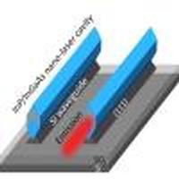
A compact, efficient, and monolithically grown III–V laser source provides an attractive alternative to bonding off-chip lasers for Si photonics research. Although recent demonstrations of microlasers on (001) Si wafers using thick metamorphic buffers are encouraging, scaling down the laser footprint to nanoscale and operating the nanolasers at telecom wavelengths remain significant challenges. Here, we report a monolithically integrated in-plane InP/InGaAs nanolaser array on (001) silicon-on-insulator (SOI) platforms with emission wavelengths covering the entire C band (1.55 μm). Multiple InGaAs quantum wells are embedded in high-quality InP nanoridges by selective-area growth on patterned (001) SOI. Combined with air-cladded InP/Si optical cavities, room-temperature operation at multiple telecom bands is obtained by defining different cavity lengths with lithography. The demonstration of telecom-wavelength monolithic nanolasers on (001) SOI platforms presents an important step towards fully integrated Si photonics circuits.
中文翻译:

在(001)绝缘体上硅上直接生长的电信InP / InGaAs纳米激光阵列
紧凑,高效且单片生长的III–V激光源为键合Si光子学研究的片外激光器提供了有吸引力的替代方法。尽管最近关于使用厚的变质缓冲液在(001)硅晶片上进行微激光演示的结果令人鼓舞,但将激光足迹缩减至纳米级并在电信波长下操作纳米激光仍然是严峻的挑战。在这里,我们报告了在(001)绝缘体上硅(SOI)平台上的单片集成式InP / InGaAs纳米激光阵列,其发射波长覆盖了整个C波段(1.55μm)。通过在图案化(001)SOI上进行选择性区域生长,将多个InGaAs量子阱嵌入高质量的InP纳米脊中。结合空气包覆的InP / Si光腔,通过使用光刻定义不同的腔长,可以获得多个电信频段的室温操作。在(001)SOI平台上的电信波长单片纳米激光器的演示为朝着完全集成的Si光子电路迈出了重要的一步。
更新日期:2019-02-15
中文翻译:
在(001)绝缘体上硅上直接生长的电信InP / InGaAs纳米激光阵列
紧凑,高效且单片生长的III–V激光源为键合Si光子学研究的片外激光器提供了有吸引力的替代方法。尽管最近关于使用厚的变质缓冲液在(001)硅晶片上进行微激光演示的结果令人鼓舞,但将激光足迹缩减至纳米级并在电信波长下操作纳米激光仍然是严峻的挑战。在这里,我们报告了在(001)绝缘体上硅(SOI)平台上的单片集成式InP / InGaAs纳米激光阵列,其发射波长覆盖了整个C波段(1.55μm)。通过在图案化(001)SOI上进行选择性区域生长,将多个InGaAs量子阱嵌入高质量的InP纳米脊中。结合空气包覆的InP / Si光腔,通过使用光刻定义不同的腔长,可以获得多个电信频段的室温操作。在(001)SOI平台上的电信波长单片纳米激光器的演示为朝着完全集成的Si光子电路迈出了重要的一步。


 京公网安备 11010802027423号