npj Flexible Electronics ( IF 12.3 ) Pub Date : 2017-09-26 , DOI: 10.1038/s41528-017-0001-1 Jung-Hun Seo , Kan Zhang , Munho Kim , Weidong Zhou , Zhenqiang Ma
|
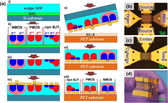
In this work, we have demonstrated for the first time integrated flexible bipolar-complementary metal-oxide-semiconductor (BiCMOS) thin-film transistors (TFTs) based on a transferable single crystalline Si nanomembrane (Si NM) on a single piece of bendable plastic substrate. The n-channel, p-channel metal-oxide semiconductor field-effect transistors (N-MOSFETs & P-MOSFETs), and NPN bipolar junction transistors (BJTs) were realized together on a 340-nm thick Si NM layer with minimized processing complexity at low cost for advanced flexible electronic applications. The fabrication process was simplified by thoughtfully arranging the sequence of necessary ion implantation steps with carefully selected energies, doses and anneal conditions, and by wisely combining some costly processing steps that are otherwise separately needed for all three types of transistors. All types of TFTs demonstrated excellent DC and radio-frequency (RF) characteristics and exhibited stable transconductance and current gain under bending conditions. Overall, Si NM-based flexible BiCMOS TFTs offer great promises for high-performance and multi-functional future flexible electronics applications and is expected to provide a much larger and more versatile platform to address a broader range of applications. Moreover, the flexible BiCMOS process proposed and demonstrated here is compatible with commercial microfabrication technology, making its adaptation to future commercial use straightforward.
中文翻译:
基于单晶硅纳米膜的高性能柔性BiCMOS电子器件
在这项工作中,我们首次展示了在单块可弯曲塑料上基于可转移单晶硅纳米膜(Si NM)的集成柔性双极互补金属氧化物半导体(BiCMOS)薄膜晶体管(TFT)基质。n沟道,p沟道金属氧化物半导体场效应晶体管(N-MOSFET和P-MOSFET)和NPN双极结晶体管(BJT)一起在厚度为340 nm的Si NM层上实现,同时将处理复杂性降至最低以低成本提供先进的柔性电子应用。通过精心安排必要的离子注入步骤的顺序以及精心选择的能量,剂量和退火条件,简化了制造过程,通过明智地组合一些昂贵的处理步骤,否则所有三种类型的晶体管都将分别需要这些处理步骤。所有类型的TFT均表现出出色的DC和射频(RF)特性,并在弯曲条件下表现出稳定的跨导和电流增益。总体而言,基于Si NM的柔性BiCMOS TFT为高性能和多功能未来的柔性电子应用提供了广阔的前景,并有望提供一个更大,更通用的平台来满足更广泛的应用。此外,此处提出和演示的灵活BiCMOS工艺与商业微细加工技术兼容,从而使其易于适应未来的商业用途。所有类型的TFT均表现出出色的DC和射频(RF)特性,并在弯曲条件下表现出稳定的跨导和电流增益。总体而言,基于Si NM的柔性BiCMOS TFT为高性能和多功能未来的柔性电子应用提供了广阔的前景,并有望提供一个更大,更通用的平台来满足更广泛的应用。此外,此处提出和演示的灵活BiCMOS工艺与商业微细加工技术兼容,从而使其易于适应未来的商业用途。所有类型的TFT均表现出出色的DC和射频(RF)特性,并在弯曲条件下表现出稳定的跨导和电流增益。总体而言,基于Si NM的柔性BiCMOS TFT为高性能和多功能未来的柔性电子应用提供了广阔的前景,并有望提供一个更大,更通用的平台来满足更广泛的应用。此外,此处提出和演示的灵活BiCMOS工艺与商业微细加工技术兼容,从而使其易于适应未来的商业用途。基于Si NM的柔性BiCMOS TFT为高性能和多功能未来的柔性电子应用提供了广阔的前景,并有望提供一个更大,更通用的平台来满足更广泛的应用。此外,此处提出和演示的灵活BiCMOS工艺与商业微细加工技术兼容,从而使其易于适应未来的商业用途。基于Si NM的柔性BiCMOS TFT为高性能和多功能未来的柔性电子应用提供了广阔的前景,并有望提供一个更大,更通用的平台来满足更广泛的应用。此外,此处提出和演示的灵活BiCMOS工艺与商业微细加工技术兼容,从而使其易于适应未来的商业用途。


 京公网安备 11010802027423号