Nature Nanotechnology ( IF 38.3 ) Pub Date : 2019-01-07 , DOI: 10.1038/s41565-018-0338-1 Matthias Koch , Joris G. Keizer , Prasanna Pakkiam , Daniel Keith , Matthew G. House , Eldad Peretz , Michelle Y. Simmons
|
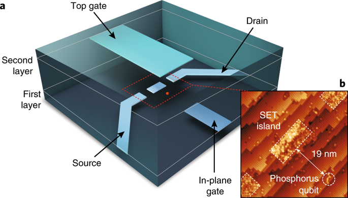
The realization of the surface code for topological error correction is an essential step towards a universal quantum computer1,2,3. For single-atom qubits in silicon4,5,6,7, the need to control and read out qubits synchronously and in parallel requires the formation of a two-dimensional array of qubits with control electrodes patterned above and below this qubit layer. This vertical three-dimensional device architecture8 requires the ability to pattern dopants in multiple, vertically separated planes of the silicon crystal with nanometre precision interlayer alignment. Additionally, the dopants must not diffuse or segregate during the silicon encapsulation. Critical components of this architecture—such as nanowires9, single-atom transistors4 and single-electron transistors10–have been realized on one atomic plane by patterning phosphorus dopants in silicon using scanning tunnelling microscope hydrogen resist lithography11,12. Here, we extend this to three dimensions and demonstrate single-shot spin read-out with 97.9% measurement fidelity of a phosphorus dopant qubit within a vertically gated single-electron transistor with <5 nm interlayer alignment accuracy. Our strategy ensures the formation of a fully crystalline transistor using just two atomic species: phosphorus and silicon.
中文翻译:
全外延三维晶体管中原子量子位的自旋读出
用于拓扑错误校正的表面代码的实现是向通用量子计算机1,2,3迈出的重要一步。对于硅4,5,6,7中的单原子量子位,需要同步且并行地控制和读出量子位,需要形成二维的量子位阵列,并在该量子位层的上方和下方构图控制电极。这种垂直的三维器件架构8需要具有以纳米级精确的层间对准在硅晶体的多个垂直分离的平面中对掺杂剂进行构图的能力。另外,在硅封装过程中,掺杂剂不得扩散或偏析。该架构的关键组件,例如纳米线9,单原子晶体管4和单电子晶体管10 –已通过使用扫描隧道显微镜氢抗蚀剂光刻技术11,12在硅中对磷掺杂剂进行构图而在一个原子平面上实现。在这里,我们将其扩展到三个维度,并演示了在垂直选通的单电子晶体管中具有小于5 nm的层间对准精度的磷掺杂量子位的97.9%的测量保真度的单次自旋读出。我们的策略可确保仅使用两种原子物质(磷和硅)形成全晶晶体管。


 京公网安备 11010802027423号