当前位置:
X-MOL 学术
›
Adv. Funct. Mater.
›
论文详情
Our official English website, www.x-mol.net, welcomes your
feedback! (Note: you will need to create a separate account there.)
Electrolyte‐Gated n‐Type Transistors Produced from Aqueous Inks of WS2 Nanosheets
Advanced Functional Materials ( IF 18.5 ) Pub Date : 2018-12-11 , DOI: 10.1002/adfm.201804387 Thomas M. Higgins 1 , Sean Finn 2 , Maik Matthiesen 1 , Sebastian Grieger 1 , Kevin Synnatschke 1 , Maximilian Brohmann 1 , Marcel Rother 1 , Claudia Backes 1 , Jana Zaumseil 1, 3
Advanced Functional Materials ( IF 18.5 ) Pub Date : 2018-12-11 , DOI: 10.1002/adfm.201804387 Thomas M. Higgins 1 , Sean Finn 2 , Maik Matthiesen 1 , Sebastian Grieger 1 , Kevin Synnatschke 1 , Maximilian Brohmann 1 , Marcel Rother 1 , Claudia Backes 1 , Jana Zaumseil 1, 3
Affiliation
|
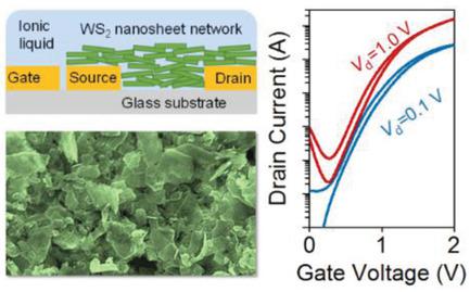
Solution‐processed, low cost thin films of layered semiconductors such as transition metal dichalcogenides (TMDs) are potential candidates for future printed electronics. Here, n‐type electrolyte‐gated transistors (EGTs) based on porous WS2 nanosheet networks as the semiconductor are demonstrated. The WS2 nanosheets are liquid phase exfoliated to form aqueous/surfactant stabilized inks, and deposited at low temperatures (T < 120 °C) in ambient atmosphere by airbrushing. No solvent exchange, further additives, or complicated processing steps are required. While the EGTs are primarily n‐type (electron accumulation), some hole transport is also observable. The EGTs show current modulations > 104 with low hysteresis, channel width‐normalized on‐conductances of up to 0.27 µS µm−1 and estimated electron mobilities around 0.01 cm2 V−1 s−1. In addition, the WS2 nanosheet networks exhibit relatively high volumetric capacitance values of 30 F cm−3. Charge transport within the network depends significantly on the applied lateral electric field and is thermally activated, which supports the notion that hopping between nanosheets is a major limiting factor for these networks and their future application.
中文翻译:

WS2纳米片的水性油墨生产的电解质门控n型晶体管
经过溶液处理的低成本多层半导体薄膜,例如过渡金属二卤化物(TMD),是未来印刷电子产品的潜在候选者。这里,展示了基于多孔WS 2纳米片网络作为半导体的n型电解质栅晶体管(EGT)。将WS 2纳米片液相剥离,以形成水/表面活性剂稳定的油墨,并通过喷枪在低温(T <120°C)下在环境气氛中沉积。无需溶剂交换,其他添加剂或复杂的处理步骤。尽管EGT主要是n型(电子积累),但也可以观察到某些空穴传输。EGT显示电流调制> 10 4具有低滞后性,通道宽度归一化导通电导高达0.27 µS µm -1,并且估计的电子迁移率约为0.01 cm 2 V -1 s -1。另外,WS 2纳米片网络表现出相对较高的30 F cm -3的体积电容值。网络中的电荷传输在很大程度上取决于所施加的横向电场并被热激活,这支持了以下观点:纳米片之间的跳跃是这些网络及其未来应用的主要限制因素。
更新日期:2018-12-11
中文翻译:
WS2纳米片的水性油墨生产的电解质门控n型晶体管
经过溶液处理的低成本多层半导体薄膜,例如过渡金属二卤化物(TMD),是未来印刷电子产品的潜在候选者。这里,展示了基于多孔WS 2纳米片网络作为半导体的n型电解质栅晶体管(EGT)。将WS 2纳米片液相剥离,以形成水/表面活性剂稳定的油墨,并通过喷枪在低温(T <120°C)下在环境气氛中沉积。无需溶剂交换,其他添加剂或复杂的处理步骤。尽管EGT主要是n型(电子积累),但也可以观察到某些空穴传输。EGT显示电流调制> 10 4具有低滞后性,通道宽度归一化导通电导高达0.27 µS µm -1,并且估计的电子迁移率约为0.01 cm 2 V -1 s -1。另外,WS 2纳米片网络表现出相对较高的30 F cm -3的体积电容值。网络中的电荷传输在很大程度上取决于所施加的横向电场并被热激活,这支持了以下观点:纳米片之间的跳跃是这些网络及其未来应用的主要限制因素。


 京公网安备 11010802027423号