Nature Nanotechnology ( IF 38.1 ) Pub Date : 2018-10-29 , DOI: 10.1038/s41565-018-0275-z Yue Luo , Gabriella D. Shepard , Jenny V. Ardelean , Daniel A. Rhodes , Bumho Kim , Katayun Barmak , James C. Hone , Stefan Strauf
|
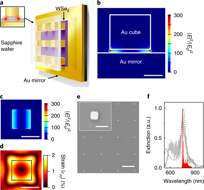
Solid-state single-quantum emitters are crucial resources for on-chip photonic quantum technologies and require efficient cavity–emitter coupling to realize quantum networks beyond the single-node level1,2. Monolayer WSe2, a transition metal dichalcogenide semiconductor, can host randomly located quantum emitters3,4,5,6, while nanobubbles7 as well as lithographically defined arrays of pillars in contact with the transition metal dichalcogenide act as spatially controlled stressors8,9. The induced strain can then create excitons at defined locations. This ability to create zero-dimensional (0D) excitons anywhere within a 2D material is promising for the development of scalable quantum technologies, but so far lacks mature cavity integration and suffers from low emitter quantum yields. Here we demonstrate a deterministic approach to achieve Purcell enhancement at lithographically defined locations using the sharp corners of a metal nanocube for both electric field enhancement and to deform a 2D material. This nanoplasmonic platform allows the study of the same quantum emitter before and after coupling. For a 3 × 4 array of quantum emitters we show Purcell factors of up to 551 (average of 181), single-photon emission rates of up to 42 MHz and a narrow exciton linewidth as low as 55 μeV. Furthermore, the use of flux-grown WSe2 increases the 0D exciton lifetimes to up to 14 ns and the cavity-enhanced quantum yields from an initial value of 1% to up to 65% (average 44%).
中文翻译:
单层WSe 2中位控量子发射体与等离子体纳米腔的确定性耦合
固态单量子发射器是片上光子量子技术的关键资源,需要有效的腔-发射极耦合才能实现超出单节点1,2的量子网络。单层WSe 2(过渡金属二卤化物半导体)可以容纳随机定位的量子发射器3、4、5、6,而纳米气泡7以及与过渡金属二卤化物接触的光刻定义的柱阵列充当空间控制的应力源8,9。。然后,诱导的应变可以在定义的位置产生激子。这种在2D材料中任何地方创建零维(0D)激子的能力对于可扩展量子技术的发展是有希望的,但是到目前为止,它缺乏成熟的腔体集成,并且发射极子的量子产率低。在这里,我们演示了一种确定性方法,该方法使用金属纳米立方体的尖角在光刻定义的位置上实现Purcell增强,从而既增强电场又使2D材料变形。该纳米等离子体平台允许在耦合之前和之后研究相同的量子发射器。对于3×4的量子发射器阵列,我们显示的赛尔因子高达551(平均181),单光子发射率高达42 MHz,窄的激子线宽低至55μeV。此外,使用助焊剂生长的WSe2使0D激子寿命增加到14 ns,腔增强量子产率从初始值的1%增长到最高的65%(平均为44%)。


 京公网安备 11010802027423号