Current Opinion in Solid State & Materials Science ( IF 12.2 ) Pub Date : 2018-09-07 , DOI: 10.1016/j.cossms.2018.09.002 Alexander S. Chang , Lincoln J. Lauhon
|
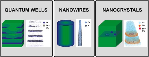
Microscopy has played a central role in the advancement of nanoscience and nanotechnology by enabling the direct visualization of nanoscale structure, leading to predictive models of novel physical behaviors. Electronic and photonic device technologies, whose features and performance are often improved through miniaturization, have particularly benefited from new capabilities in the characterization of material structure and composition. This paper reviews recent applications of atom probe tomography to semiconducting materials with nanoscale architectures that are designed to impart novel properties and device functionality by virtue of their shape and size. A review is necessary because rapid advances in atom probe instrumentation and analysis in the last decade have greatly expanded the utility of atom probe tomography to address scientific questions and technical questions in this area. The paper is organized in terms of the surface topologies of nanoscale architectures. We begin with nominally planar interfaces including thin film heterostructures and superlattices with open surfaces. Distinctive capabilities in the analysis of interfaces are introduced, as are challenges arising from measurement artifacts. We then discuss nanowires and nanowire heterostructures with surfaces that are closed along one dimension, for which atom probe tomography has provided unique and important understandings on the doping processes. Finally, we consider nanocrystals and quantum dots with completely closed surfaces. Along the way, current challenges and opportunities for atom probe tomography are highlighted, and the reader is directed to complementary reviews of more technical aspects of atom probe analysis.
中文翻译:
电子和光子应用功能材料中纳米结构的原子探针层析成像
显微镜技术通过直接可视化纳米尺度结构,从而为新型物理行为的预测模型,在纳米科学和纳米技术的发展中发挥了核心作用。电子和光子器件技术的特征和性能通常通过小型化得到改善,特别受益于表征材料结构和成分的新功能。本文回顾了原子探针层析成像技术在具有纳米级结构的半导体材料上的最新应用,这些材料被设计成凭借其形状和尺寸来赋予新颖的特性和器件功能。回顾是必要的,因为在过去十年中,原子探针仪器和分析技术的快速发展极大地扩展了原子探针层析成像技术在解决这一领域中的科学问题和技术问题方面的实用性。本文根据纳米级体系结构的表面拓扑进行组织。我们从名义上的平面界面开始,包括薄膜异质结构和具有开放表面的超晶格。引入了界面分析中的独特功能,以及测量工件带来的挑战。然后,我们讨论了沿一维闭合表面的纳米线和纳米线异质结构,为此,原子探针层析成像技术对掺杂过程提供了独特而重要的理解。最后,我们考虑具有完全封闭表面的纳米晶体和量子点。在此过程中,重点介绍了原子探针层析成像技术的当前挑战和机遇,并向读者介绍了原子探针分析更多技术方面的补充评论。


 京公网安备 11010802027423号