Our official English website, www.x-mol.net, welcomes your
feedback! (Note: you will need to create a separate account there.)
Characteristics of graphene grown through low power capacitive coupled radio frequency plasma enhanced chemical vapor deposition
Carbon ( IF 10.5 ) Pub Date : 2020-04-01 , DOI: 10.1016/j.carbon.2019.12.093 Yu-Chen Chang , Chun-Chieh Yen , Hung-Chieh Tsai , Tsung Cheng Chen , Chia-Ming Yang , Chia-Hao Chen , Wei-Yen Woon
Carbon ( IF 10.5 ) Pub Date : 2020-04-01 , DOI: 10.1016/j.carbon.2019.12.093 Yu-Chen Chang , Chun-Chieh Yen , Hung-Chieh Tsai , Tsung Cheng Chen , Chia-Ming Yang , Chia-Hao Chen , Wei-Yen Woon
|
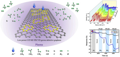
Abstract We study the characteristics of graphene grown through low power capacitive coupled radio frequency plasma enhanced chemical vapor deposition (PECVD) and explore its application. Fully-covered, mostly single-layered, and highly defective graphene films were grown on Cu substrates through plasma composed of various argon/methane/hydrogen gas ratio with low RF power within a minute under a moderate substrate temperature at 850 °C . The structural, chemical, and electrical properties of the graphene films were measured through Raman spectroscopy, X-ray photoelectron spectroscopy, and Hall measurement, respectively. The Raman signatures were strongly affected by the argon/hydrogen flow rates and the subsequent thermal annealing, and is strongly correlated to carrier mobility of the film. Through analysis of the defect related Raman bands within the theoretical framework of activated defect model, it is concluded that the defects found in the graphene films are originated from ion bombardment during the growth processes. The vacancy defects on the graphene film provides adsorption sites for gaseous molecules and induces changes of charge transfer in the graphene film. The response of the graphene-based sensor fabricated with the PECVD grown graphene is 6% under 100 ppb of N O 2 , which can be a candidate of potential N O 2 gas sensing material in the future.
中文翻译:

低功率电容耦合射频等离子体增强化学气相沉积生长石墨烯的特性
摘要 我们研究了通过低功率电容耦合射频等离子体增强化学气相沉积(PECVD)生长的石墨烯的特性并探索其应用。在 850 °C 的中等衬底温度下,通过由各种氩/甲烷/氢气比例组成的等离子体在 1 分钟内以低 RF 功率在 Cu 衬底上生长完全覆盖、主要是单层和高度缺陷的石墨烯薄膜。石墨烯薄膜的结构、化学和电学性质分别通过拉曼光谱、X 射线光电子能谱和霍尔测量进行测量。拉曼特征受到氩气/氢气流速和随后的热退火的强烈影响,并且与薄膜的载流子迁移率密切相关。通过在激活缺陷模型的理论框架内分析缺陷相关的拉曼带,得出结论,石墨烯薄膜中发现的缺陷源于生长过程中的离子轰击。石墨烯薄膜上的空位缺陷为气态分子提供了吸附位点,并引起石墨烯薄膜中电荷转移的变化。使用PECVD 生长的石墨烯制造的石墨烯基传感器在100 ppb NO 2 下的响应为6%,可以成为未来潜在的NO 2 气敏材料的候选者。石墨烯薄膜上的空位缺陷为气态分子提供了吸附位点,并引起石墨烯薄膜中电荷转移的变化。用PECVD 生长的石墨烯制造的石墨烯基传感器在100 ppb NO 2 下的响应为6%,可以成为未来潜在的NO 2 气敏材料的候选者。石墨烯薄膜上的空位缺陷为气态分子提供了吸附位点,并引起石墨烯薄膜中电荷转移的变化。用PECVD 生长的石墨烯制造的石墨烯基传感器在100 ppb NO 2 下的响应为6%,可以成为未来潜在的NO 2 气敏材料的候选者。
更新日期:2020-04-01
中文翻译:
低功率电容耦合射频等离子体增强化学气相沉积生长石墨烯的特性
摘要 我们研究了通过低功率电容耦合射频等离子体增强化学气相沉积(PECVD)生长的石墨烯的特性并探索其应用。在 850 °C 的中等衬底温度下,通过由各种氩/甲烷/氢气比例组成的等离子体在 1 分钟内以低 RF 功率在 Cu 衬底上生长完全覆盖、主要是单层和高度缺陷的石墨烯薄膜。石墨烯薄膜的结构、化学和电学性质分别通过拉曼光谱、X 射线光电子能谱和霍尔测量进行测量。拉曼特征受到氩气/氢气流速和随后的热退火的强烈影响,并且与薄膜的载流子迁移率密切相关。通过在激活缺陷模型的理论框架内分析缺陷相关的拉曼带,得出结论,石墨烯薄膜中发现的缺陷源于生长过程中的离子轰击。石墨烯薄膜上的空位缺陷为气态分子提供了吸附位点,并引起石墨烯薄膜中电荷转移的变化。使用PECVD 生长的石墨烯制造的石墨烯基传感器在100 ppb NO 2 下的响应为6%,可以成为未来潜在的NO 2 气敏材料的候选者。石墨烯薄膜上的空位缺陷为气态分子提供了吸附位点,并引起石墨烯薄膜中电荷转移的变化。用PECVD 生长的石墨烯制造的石墨烯基传感器在100 ppb NO 2 下的响应为6%,可以成为未来潜在的NO 2 气敏材料的候选者。石墨烯薄膜上的空位缺陷为气态分子提供了吸附位点,并引起石墨烯薄膜中电荷转移的变化。用PECVD 生长的石墨烯制造的石墨烯基传感器在100 ppb NO 2 下的响应为6%,可以成为未来潜在的NO 2 气敏材料的候选者。


 京公网安备 11010802027423号