当前位置:
X-MOL 学术
›
Nano Lett.
›
论文详情
Our official English website, www.x-mol.net, welcomes your feedback! (Note: you will need to create a separate account there.)
Operando Surface Characterization of InP Nanowire p-n Junctions.
Nano Letters ( IF 10.8 ) Pub Date : 2020-01-08 , DOI: 10.1021/acs.nanolett.9b03529 Sarah R McKibbin 1 , Jovana Colvin 1 , Andrea Troian 1 , Johan V Knutsson 1 , James L Webb 1 , Gaute Otnes 1 , Kai Dirscherl 2 , Hikmet Sezen 3 , Matteo Amati 3 , Luca Gregoratti 3 , Magnus T Borgström 1 , Anders Mikkelsen 1 , Rainer Timm 1
Nano Letters ( IF 10.8 ) Pub Date : 2020-01-08 , DOI: 10.1021/acs.nanolett.9b03529 Sarah R McKibbin 1 , Jovana Colvin 1 , Andrea Troian 1 , Johan V Knutsson 1 , James L Webb 1 , Gaute Otnes 1 , Kai Dirscherl 2 , Hikmet Sezen 3 , Matteo Amati 3 , Luca Gregoratti 3 , Magnus T Borgström 1 , Anders Mikkelsen 1 , Rainer Timm 1
Affiliation
|
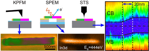
We present an in-depth analysis of the surface band alignment and local potential distribution of InP nanowires containing a p-n junction using scanning probe and photoelectron microscopy techniques. The depletion region is localized to a 15 nm thin surface region by scanning tunneling spectroscopy and an electronic shift of up to 0.5 eV between the n- and p-doped nanowire segments was observed and confirmed by Kelvin probe force microscopy. Scanning photoelectron microscopy then allowed us to measure the intrinsic chemical shift of the In 3d, In 4d, and P 2p core level spectra along the nanowire and the effect of operating the nanowire diode in forward and reverse bias on these shifts. Thanks to the high-resolution techniques utilized, we observe fluctuations in the potential and chemical energy of the surface along the nanowire in great detail, exposing the sensitive nature of nanodevices to small scale structural variations.
中文翻译:

InP纳米线pn结的Operando表面表征。
我们提出了使用扫描探针和光电子显微镜技术对包含pn结的InP纳米线的表面能带对准和局部电势分布进行深入分析。通过扫描隧穿光谱法将耗尽区定位在15nm的薄表面区域,并且在开尔文探针力显微镜下观察到并确认了在n-和p-掺杂的纳米线段之间高达0.5eV的电子位移。扫描光电子显微镜随后使我们能够测量沿纳米线的In 3d,In 4d和P 2p核能级谱的固有化学位移,以及在这些位移上正向和反向偏置下操作纳米线二极管的效果。由于采用了高分辨率技术,我们可以非常详细地观察到沿着纳米线的表面电势和化学能的波动,
更新日期:2020-01-09
中文翻译:
InP纳米线pn结的Operando表面表征。
我们提出了使用扫描探针和光电子显微镜技术对包含pn结的InP纳米线的表面能带对准和局部电势分布进行深入分析。通过扫描隧穿光谱法将耗尽区定位在15nm的薄表面区域,并且在开尔文探针力显微镜下观察到并确认了在n-和p-掺杂的纳米线段之间高达0.5eV的电子位移。扫描光电子显微镜随后使我们能够测量沿纳米线的In 3d,In 4d和P 2p核能级谱的固有化学位移,以及在这些位移上正向和反向偏置下操作纳米线二极管的效果。由于采用了高分辨率技术,我们可以非常详细地观察到沿着纳米线的表面电势和化学能的波动,


 京公网安备 11010802027423号