Our official English website, www.x-mol.net, welcomes your
feedback! (Note: you will need to create a separate account there.)
Antenna-coupled vacuum channel nano-diode with high quantum efficiency.
Nanoscale ( IF 5.8 ) Pub Date : 2020-01-08 , DOI: 10.1039/c9nr06109f Shenghan Zhou 1 , Ke Chen , Xiangdong Guo , Matthew Thomas Cole , Yu Wu , Zhenjun Li , Shunping Zhang , Chi Li , Qing Dai
Nanoscale ( IF 5.8 ) Pub Date : 2020-01-08 , DOI: 10.1039/c9nr06109f Shenghan Zhou 1 , Ke Chen , Xiangdong Guo , Matthew Thomas Cole , Yu Wu , Zhenjun Li , Shunping Zhang , Chi Li , Qing Dai
Affiliation
|
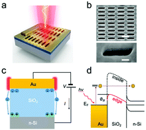
Vacuum channel diodes have the potential to serve as a platform for converting free-space electromagnetic radiation into electronic signals within ultrafast timescales. However, the conversion efficiency is typically very low because conventional vacuum channel diode structures suffer from high surface barriers, especially when using lower energy photon excitation (near-infrared photons or lower). Here, we report on an optical antenna-coupled vacuum channel nano-diode, which demonstrates a greatly improved quantum efficiency up to ∼4% at 800 nm excitation; an efficiency several orders of magnitude higher than any previously reported value. The nano diodes are formed at the cleaved edge of a metal-insulator-semiconductor (MIS) structure, where a gold thin film with nanohole array serves as both the metal electrode and light-harvesting antenna. At the nanoholes-insulator interface, the tunneling barrier is greatly reduced due to the coulombic repulsion induced high local electron density, such that the resonant plasmon induced hot electron population can readily inject into the vacuum channel. The presented vertical tertiary MIS junction enables a new class of high-efficiency, polarization-specific and wavelength- sensitive optical modulated photodetector that has the potential for developing a new generation of opto-electronic systems.
中文翻译:

具有高量子效率的天线耦合真空通道纳米二极管。
真空通道二极管有潜力用作在超快时间范围内将自由空间电磁辐射转换为电子信号的平台。但是,转换效率通常非常低,因为常规的真空沟道二极管结构会受到较高的表面势垒的影响,尤其是在使用较低能量的光子激发(近红外光子或更低的光子)时。在这里,我们报道了一种与光天线耦合的真空通道纳米二极管,该二极管在800 nm激发下显示出高达4%的量子效率。效率比以前报告的值高几个数量级。纳米二极管形成在金属-绝缘体-半导体(MIS)结构的开裂边缘处,其中具有纳米孔阵列的金薄膜既充当金属电极又充当光收集天线。在纳米孔-绝缘体界面处,由于库仑排斥引起的高局部电子密度而大大减小了隧穿势垒,从而使共振等离子体激元引起的热电子种群可以容易地注入真空通道。提出的垂直三级MIS结实现了新型的高效,偏振特定和对波长敏感的光调制光电探测器,具有开发新一代光电系统的潜力。
更新日期:2020-01-08
中文翻译:
具有高量子效率的天线耦合真空通道纳米二极管。
真空通道二极管有潜力用作在超快时间范围内将自由空间电磁辐射转换为电子信号的平台。但是,转换效率通常非常低,因为常规的真空沟道二极管结构会受到较高的表面势垒的影响,尤其是在使用较低能量的光子激发(近红外光子或更低的光子)时。在这里,我们报道了一种与光天线耦合的真空通道纳米二极管,该二极管在800 nm激发下显示出高达4%的量子效率。效率比以前报告的值高几个数量级。纳米二极管形成在金属-绝缘体-半导体(MIS)结构的开裂边缘处,其中具有纳米孔阵列的金薄膜既充当金属电极又充当光收集天线。在纳米孔-绝缘体界面处,由于库仑排斥引起的高局部电子密度而大大减小了隧穿势垒,从而使共振等离子体激元引起的热电子种群可以容易地注入真空通道。提出的垂直三级MIS结实现了新型的高效,偏振特定和对波长敏感的光调制光电探测器,具有开发新一代光电系统的潜力。


 京公网安备 11010802027423号