Applied Materials Today ( IF 7.2 ) Pub Date : 2019-12-23 , DOI: 10.1016/j.apmt.2019.100532 Zhipeng Yan , Ketao Yin , Zhenhai Yu , Xin Li , Mingtao Li , Ye Yuan , Xiaodong Li , Ke Yang , Xiaoli Wang , Lin Wang
|
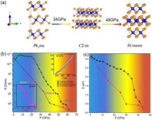
In this letter, we present the pressure-induced evolution of the band-gap, conductance, and crystal structure of layered transition metal dihalide (TMH), CdI2, an insulator at ambient conditions, using electrical transport measurement, UV–vis absorption spectroscopy, X-ray diffraction, and Raman scattering spectroscopy. We found that the band gap shrinks gradually following a sharp drop at 34.5 GPa. Meanwhile, the temperature-dependent resistance indicated an insulator-to-semiconductor and then metal transition occurred at 36 and 62 GPa, respectively. Both X-ray diffraction and Raman scattering measurements indicate that the CdI2 underwent a first-order transition from a hexagonal to monoclinic phase at ∼32 GPa due to collapses in the c-lattice parameter and volume. The second structural phase transition (SPT) from monoclinic-to-tetragonal occurred at 48 GPa. The pressure-induced insulator-to-semiconductor-to-metal of CdI2 is attributed to the structural transition from hexagonal-to-monoclinic-to-tetragonal. Our first-principle calculations further confirm the sequence of the SPTs and the semiconducting and metallic band structure of the phases, respectively. Namely, the metallization is observed due to the filled 5p-iodide to shift and overlap with the filled 5s-cadmium band in metal phase. These findings pave the way for investigating crystal structure evolution, and the optical and electrical properties in CdI2-type compounds under extreme conditions.
中文翻译:
二维过渡金属卤化物CdI 2中的压力诱导带隙封闭和金属化
在这封信中,我们介绍了在环境条件下使用电迁移测量,紫外可见吸收光谱法对层状过渡金属二卤化物(TMH)CdI 2(绝缘子)的带隙,电导和晶体结构进行压力诱导的演化的过程。,X射线衍射和拉曼散射光谱。我们发现,带隙在34.5 GPa急剧下降之后逐渐减小。同时,取决于温度的电阻指示绝缘体到半导体,然后分别在36 GPa和62 GPa处发生金属转变。X射线衍射和拉曼散射测量均表明CdI 2在约32 GPa处经历了从六方相到单斜晶相的一阶跃迁,这是由于c的塌陷所致。-晶格参数和体积。从单斜向四方的第二个结构相变(SPT)发生在48 GPa。CdI 2的压力诱导的绝缘体到半导体到金属的归因于从六边形到单斜晶到四边形的结构转变。我们的第一性原理计算进一步确定了SPT的顺序以及各相的半导体和金属能带结构。即,观察到金属化是由于填充的5p-碘在金属相中移动并与填充的5s-镉带重叠。这些发现为研究晶体结构演变以及在极端条件下CdI 2型化合物的光学和电学性质铺平了道路。


 京公网安备 11010802027423号