当前位置:
X-MOL 学术
›
Nano Lett.
›
论文详情
Our official English website, www.x-mol.net, welcomes your
feedback! (Note: you will need to create a separate account there.)
Quantitative Nanoscale Absorption Mapping: A Novel Technique To Probe Optical Absorption of Two-Dimensional Materials.
Nano Letters ( IF 9.6 ) Pub Date : 2019-12-27 , DOI: 10.1021/acs.nanolett.9b04304 Marco Negri 1 , Luca Francaviglia 1 , Dumitru Dumcenco 1, 2 , Matteo Bosi 3 , Daniel Kaplan 4 , Venkataraman Swaminathan 4 , Giancarlo Salviati 3 , Andras Kis 2 , Filippo Fabbri 5 , Anna Fontcuberta I Morral 1, 6
Nano Letters ( IF 9.6 ) Pub Date : 2019-12-27 , DOI: 10.1021/acs.nanolett.9b04304 Marco Negri 1 , Luca Francaviglia 1 , Dumitru Dumcenco 1, 2 , Matteo Bosi 3 , Daniel Kaplan 4 , Venkataraman Swaminathan 4 , Giancarlo Salviati 3 , Andras Kis 2 , Filippo Fabbri 5 , Anna Fontcuberta I Morral 1, 6
Affiliation
|
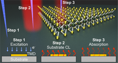
Two-dimensional semiconductors, in particular transition metal dichalcogenides and related heterostructures, have gained increasing interest as they constitute potential new building blocks for the next generation of electronic and optoelectronic applications. In this work, we develop a novel nondestructive and noncontact technique for mapping the absorption properties of 2D materials, by taking advantage of the underlying substrate cathodoluminescence emission. We map the quantitative absorption of MoS2 and MoSe2 monolayers, obtained on sapphire and oxidized silicon, with nanoscale resolution. We extend our technique to the characterization of the absorption properties of MoS2/MoSe2 van der Waals heterostructures. We demonstrate that interlayer excitonic phenomena enhance the absorption in the UV range. Our technique also highlights the presence of defects such as grain boundaries and ad-layers. We provide measurements on the absorption of grain boundaries in monolayer MoS2 at different merging angles. We observe a higher absorption yield of randomly oriented monolayers with respect to 60° rotated monolayers. This work opens up a new possibility for characterizing the functional properties two-dimensional semiconductors at the nanoscale.
中文翻译:

定量纳米尺度吸收图:探测二维材料光学吸收的新技术。
二维半导体,尤其是过渡金属二硫属化合物和相关的异质结构,由于它们构成了下一代电子和光电应用的潜在新构件,因此引起了越来越多的关注。在这项工作中,我们开发了一种新颖的非破坏性和非接触性技术,通过利用底层衬底的阴极发光发光来绘制2D材料的吸收特性。我们绘制了在蓝宝石和氧化硅上获得的纳米级分辨率的MoS2和MoSe2单层的定量吸收图。我们将技术扩展到MoS2 / MoSe2 van der Waals异质结构的吸收特性的表征。我们证明了层间激子现象增强了UV范围内的吸收。我们的技术还强调了缺陷的存在,例如晶界和广告层。我们提供了在不同合并角度下单层MoS2中晶界吸收的测量。我们观察到随机取向的单分子层相对于60°旋转的单分子层的吸收率更高。这项工作为表征纳米级二维半导体的功能特性开辟了新的可能性。
更新日期:2019-12-29
中文翻译:
定量纳米尺度吸收图:探测二维材料光学吸收的新技术。
二维半导体,尤其是过渡金属二硫属化合物和相关的异质结构,由于它们构成了下一代电子和光电应用的潜在新构件,因此引起了越来越多的关注。在这项工作中,我们开发了一种新颖的非破坏性和非接触性技术,通过利用底层衬底的阴极发光发光来绘制2D材料的吸收特性。我们绘制了在蓝宝石和氧化硅上获得的纳米级分辨率的MoS2和MoSe2单层的定量吸收图。我们将技术扩展到MoS2 / MoSe2 van der Waals异质结构的吸收特性的表征。我们证明了层间激子现象增强了UV范围内的吸收。我们的技术还强调了缺陷的存在,例如晶界和广告层。我们提供了在不同合并角度下单层MoS2中晶界吸收的测量。我们观察到随机取向的单分子层相对于60°旋转的单分子层的吸收率更高。这项工作为表征纳米级二维半导体的功能特性开辟了新的可能性。


 京公网安备 11010802027423号