当前位置:
X-MOL 学术
›
Chem. Mater.
›
论文详情
Our official English website, www.x-mol.net, welcomes your
feedback! (Note: you will need to create a separate account there.)
Structure–Charge Transport Relationships in Fluoride-Doped Amorphous Semiconducting Indium Oxide: Combined Experimental and Theoretical Analysis
Chemistry of Materials ( IF 7.2 ) Pub Date : 2020-01-08 , DOI: 10.1021/acs.chemmater.9b04257 Aritra Sil , Laleh Avazpour 1 , Elise A. Goldfine , Qing Ma 2 , Wei Huang , Binghao Wang , Michael J. Bedzyk , Julia E. Medvedeva 1 , Antonio Facchetti 3 , Tobin J. Marks
Chemistry of Materials ( IF 7.2 ) Pub Date : 2020-01-08 , DOI: 10.1021/acs.chemmater.9b04257 Aritra Sil , Laleh Avazpour 1 , Elise A. Goldfine , Qing Ma 2 , Wei Huang , Binghao Wang , Michael J. Bedzyk , Julia E. Medvedeva 1 , Antonio Facchetti 3 , Tobin J. Marks
Affiliation
|
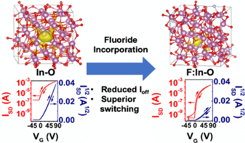
Anion doping of transparent amorphous metal oxide (a-MO) semiconductors is virtually unexplored but offers the possibility of creating unique optoelectronic materials owing to the chemical tuning, modified crystal structures, and unusual charge-transport properties that added anions may impart. We report here the effects of fluoride (F–) doping by combustion synthesis, in an archetypical metal oxide semiconductor, indium oxide (In–O). Optimized fluoride-doped In–O (F:In–O) thin films are characterized in depth by grazing incidence X-ray diffraction, X-ray reflectivity, atomic force microscopy, X-ray photoelectron spectroscopy, and extended X-ray absorption fine structure (EXAFS). Charge-transport properties are investigated in thin-film transistors (TFTs), revealing that increasing fluoride content (0.0 → 1.57 atom %) slightly lowers the on-current (Ion) and electron mobility due to scattering from loosely bound F– centers but enhances important TFT performance parameters such as the Ion/Ioff ratio, subthreshold swing, and bias stress stability, yielding superior TFT switching versus undoped In–O. These results are convincingly explained by ab initio molecular dynamics simulations and density functional theory electronic structure calculations. Combined with the EXAFS data, the experimental and theoretical results show that F– hinders crystallization by enhancing the local and medium-range disorder, promotes a uniform film morphology, and favors the formation of deeper, more localized trap states as compared to F–-free In–O. These data also show that the local organization and electronic structure of amorphous F–-doped oxide semiconductors are significantly different from those of F–-doped crystalline oxide semiconductors and suggest new avenues to further modify a-MOs for enhanced optoelectronic properties.
中文翻译:

掺氟非晶半导体氧化铟的结构电荷传输关系:组合的实验和理论分析
透明无定形金属氧化物(a-MO)半导体的阴离子掺杂实际上尚未开发,但由于化学调谐,修饰的晶体结构以及添加的阴离子可能赋予的异常电荷传输特性,因此提供了创建独特的光电材料的可能性。我们在这里报告氟化物的影响(F –)通过燃烧合成在典型的金属氧化物半导体中掺杂氧化铟(In-O)。优化的氟化物掺杂的In-O(F:In-O)薄膜在深度上具有掠入射X射线衍射,X射线反射率,原子力显微镜,X射线光电子能谱和扩展的X射线吸收特性。结构(EXAFS)。在薄膜晶体管(TFT)的电荷传输性能进行了研究,揭示了增加氟含量(0.0→1.57原子%)略微降低导通电流(我上)和电子迁移率由于从松散结合˚F散射-中心但增强重要的TFT性能参数,例如I on / I off比率,亚阈值摆幅和偏置应力稳定性,与未掺杂的In-O相比,可产生出众的TFT开关。从头算分子动力学模拟和密度泛函理论电子结构计算可以令人信服地解释这些结果。与EXAFS数据相结合,实验和理论结果表明那个F -阻碍结晶通过增强本地和中程障碍,促进均匀的膜的形态,并且与到F有利于更深,更局部化陷阱态的形成- -免费的In-O。这些数据还表明,无定形F中的本地组织和电子结构-掺杂的氧化半导体与那些的F显著不同-掺杂的晶体氧化物半导体,并提出了新的途径来进一步修饰a-MO,以增强光电性能。
更新日期:2020-01-08
中文翻译:
掺氟非晶半导体氧化铟的结构电荷传输关系:组合的实验和理论分析
透明无定形金属氧化物(a-MO)半导体的阴离子掺杂实际上尚未开发,但由于化学调谐,修饰的晶体结构以及添加的阴离子可能赋予的异常电荷传输特性,因此提供了创建独特的光电材料的可能性。我们在这里报告氟化物的影响(F –)通过燃烧合成在典型的金属氧化物半导体中掺杂氧化铟(In-O)。优化的氟化物掺杂的In-O(F:In-O)薄膜在深度上具有掠入射X射线衍射,X射线反射率,原子力显微镜,X射线光电子能谱和扩展的X射线吸收特性。结构(EXAFS)。在薄膜晶体管(TFT)的电荷传输性能进行了研究,揭示了增加氟含量(0.0→1.57原子%)略微降低导通电流(我上)和电子迁移率由于从松散结合˚F散射-中心但增强重要的TFT性能参数,例如I on / I off比率,亚阈值摆幅和偏置应力稳定性,与未掺杂的In-O相比,可产生出众的TFT开关。从头算分子动力学模拟和密度泛函理论电子结构计算可以令人信服地解释这些结果。与EXAFS数据相结合,实验和理论结果表明那个F -阻碍结晶通过增强本地和中程障碍,促进均匀的膜的形态,并且与到F有利于更深,更局部化陷阱态的形成- -免费的In-O。这些数据还表明,无定形F中的本地组织和电子结构-掺杂的氧化半导体与那些的F显著不同-掺杂的晶体氧化物半导体,并提出了新的途径来进一步修饰a-MO,以增强光电性能。


 京公网安备 11010802027423号