Science Bulletin ( IF 18.8 ) Pub Date : 2019-12-20 , DOI: 10.1016/j.scib.2019.12.018 Dong Li 1 , Chenguang Zhu 1 , Huawei Liu 1 , Xingxia Sun 1 , Biyuan Zheng 1 , Ying Liu 1 , Yong Liu 1 , Xingwang Wang 1 , Xiaoli Zhu 1 , Xiao Wang 1 , Anlian Pan 1
|
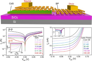
The realization of light-triggered devices where light is used as external stimulus to control the device performances is a long-standing goal in modern opto-electrical interconnection circuits. In this work, it reveals that light illumination can induce the formation of p-n junctions along two-dimensional conduction channels. The results indicate that the dominant charge carrier type and density in black phosphorus (BP) conduction channel can be effectively modulated by the underlying cadmium sulfide (CdS) photo-gate layer under light illumination. This enables flexible switching of the working state between BP resistor and BP p-n diode in the designed semi-photo-gate transistor (SPGT) devices when switching the light on and off (ultra-low threshold light power). Simultaneously, the achieved BP p-n junctions also exhibit ultra-high photoresponsivity and evident photovoltaic properties. That is to say, light can be employed as external stimulus to define the BP p-n junctions, and in turn the p-n junctions will further convert the light into electrical power, showing all-in-one opto-electrical interconnection properties. Moreover, the SPGT device architecture is also applicable for construction of other ambipolar semiconductor-based (WSe2- and MoTe2-based) p-n diodes. Such universal all-in-one light-triggered lateral homogeneous p-n junctions with ultra-low energy consumption should open a new pathway toward novel optoelectronic devices and deliver various new applications.
中文翻译:
光电互连电路用光触发二维横向同质pn二极管
实现将光用作外部刺激来控制器件性能的光触发器件是现代光电互连电路的长期目标。在这项工作中,它表明光照可以诱导沿二维传导通道形成 pn 结。结果表明,在光照下,底层硫化镉 (CdS) 光栅层可以有效地调制黑磷 (BP) 传导通道中的主要电荷载流子类型和密度。这使得在打开和关闭光(超低阈值光功率)时,设计的半光栅晶体管(SPGT)器件中的 BP 电阻和 BP pn 二极管之间的工作状态可以灵活切换。同时,所实现的 BP pn 结还表现出超高的光响应性和明显的光伏特性。也就是说,光可以作为外部刺激来定义BP pn结,而pn结又会将光进一步转化为电能,表现出一体化的光电互连特性。此外,SPGT 器件架构还适用于构建其他基于双极半导体(WSe2 - 和 MoTe 2基)pn 二极管。这种具有超低能耗的通用一体式光触发横向均匀 pn 结应该为新型光电器件开辟一条新途径,并提供各种新应用。


 京公网安备 11010802027423号