Science Bulletin ( IF 18.8 ) Pub Date : 2019-12-16 , DOI: 10.1016/j.scib.2019.12.015 Kailun Xia 1 , Wenqiang Wu 2 , Mengjia Zhu 1 , Xinyi Shen 3 , Zhe Yin 1 , Haomin Wang 1 , Shuo Li 1 , Mingchao Zhang 1 , Huimin Wang 1 , Haojie Lu 1 , Anlian Pan 4 , Caofeng Pan 5 , Yingying Zhang 1
|
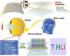
Hybrid perovskite possesses excellent photoelectric properties, including large light-absorption capacity and high carrier mobility, and is an ideal light-absorbing material for photoelectric devices. The grain size and compactness of hybrid perovskite are key factors affecting the performance of photoelectric devices. The photocurrent and photoresponsivity of these devices are relatively low because of the rapidly recombined photoexcited electron-hole pairs in hybrid perovskite. Herein, we develop a facile two-step chemical vapor deposition (CVD) method to synthesize a high-quality van der Waals (vdWs) MAPbI3/graphene heterostructure for high-performance image sensor. We introduced inorganic sources (PbI2) to vdWs epitaxially grown PbI2 film on a seamless graphene monolayer film template through CVD. Methylammonium iodide (MAI) was then reintroduced to prepare the vdWs MAPbI3/graphene heterostructure. The MAPbI3 layer is composed of densely packed, large-size grains and displays a smooth surface. High photoresponsivity of 107 A/W is achieved in the corresponding photodetector. Inspired by the human visual system, we designed a flexible photodetector array containing (24×24) pixels, achieving perfect image recognition and color discrimination. Our study may greatly facilitate the construction of high-performance optoelectronic devices in artificial retina, biomedical imaging, remote sensing, and optical communication.
中文翻译:
用于高性能柔性图像传感器的钙钛矿/石墨烯薄膜的 CVD 生长
杂化钙钛矿具有优异的光电性能,包括大的光吸收容量和高载流子迁移率,是用于光电器件的理想光吸收材料。杂化钙钛矿的晶粒尺寸和致密性是影响光电器件性能的关键因素。由于杂化钙钛矿中快速重组的光激发电子-空穴对,这些器件的光电流和光响应性相对较低。在此,我们开发了一种简便的两步化学气相沉积 (CVD) 方法来合成用于高性能图像传感器的高质量范德华 (vdWs) MAPbI 3 /石墨烯异质结构。我们将无机源 ( PbI 2 ) 引入到 vdWs 外延生长的 PbI 2中通过 CVD 在无缝石墨烯单层膜模板上形成薄膜。然后重新引入甲基碘化铵 (MAI) 以制备 vdWs MAPbI 3 /石墨烯异质结构。MAPbI 3层由致密的大尺寸晶粒组成,表面光滑。在相应的光电探测器中实现了10 7 A/W 的高光响应性。受人类视觉系统的启发,我们设计了一个包含(24×24)像素的柔性光电探测器阵列,实现了完美的图像识别和颜色辨别。我们的研究可能极大地促进人工视网膜、生物医学成像、遥感和光通信中高性能光电器件的构建。


 京公网安备 11010802027423号