npj 2D Materials and Applications ( IF 9.1 ) Pub Date : 2019-12-13 , DOI: 10.1038/s41699-019-0133-3 Yi-Hsun Chen , Chih-Yi Cheng , Shao-Yu Chen , Jan Sebastian Dominic Rodriguez , Han-Ting Liao , Kenji Watanabe , Takashi Taniguchi , Chun-Wei Chen , Raman Sankar , Fang-Cheng Chou , Hsiang-Chih Chiu , Wei-Hua Wang
|
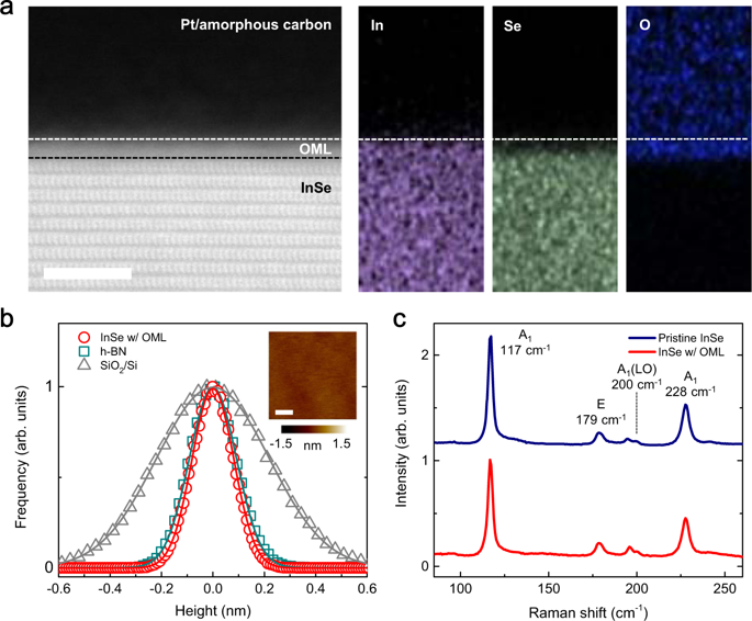
In two-dimensional (2D)-semiconductor-based field-effect transistors and optoelectronic devices, metal–semiconductor junctions are one of the crucial factors determining device performance. The Fermi-level (FL) pinning effect, which commonly caused by interfacial gap states, severely limits the tunability of junction characteristics, including barrier height and contact resistance. A tunneling contact scheme has been suggested to address the FL pinning issue in metal–2D-semiconductor junctions, whereas the experimental realization is still elusive. Here, we show that an oxidized-monolayer-enabled tunneling barrier can realize a pronounced FL depinning in indium selenide (InSe) transistors, exhibiting a large pinning factor of 0.5 and a highly modulated Schottky barrier height. The FL depinning can be attributed to the suppression of metal- and disorder-induced gap states as a result of the high-quality tunneling contacts. Structural characterizations indicate uniform and atomically thin-surface oxidation layer inherent from nature of van der Waals materials and atomically sharp oxide–2D-semiconductor interfaces. Moreover, by effectively lowering the Schottky barrier height, we achieve an electron mobility of 2160 cm2/Vs and a contact barrier of 65 meV in two-terminal InSe transistors. The realization of strong FL depinning in high-mobility InSe transistors with the oxidized-monolayer presents a viable strategy to exploit layered semiconductors in contact engineering for advanced electronics and optoelectronics.
中文翻译:
氧化单层隧穿势垒可在层状InSe晶体管中实现强费米能级钉扎
在基于二维(2D)半导体的场效应晶体管和光电器件中,金属-半导体结是决定器件性能的关键因素之一。通常由界面间隙状态引起的费米能级(FL)钉扎效应严重限制了结特性(包括势垒高度和接触电阻)的可调性。已经提出了一种隧道接触方案来解决金属2D半导体结中的FL钉扎问题,而实验实现仍是可望而不可及的。在这里,我们显示了启用了氧化单层的隧穿势垒可以实现硒化铟(InSe)晶体管中的显着FL钉扎,展现出0.5的大钉扎因子和高度调制的肖特基势垒高度。FL脱钉可归因于高质量隧穿接触的抑制金属和无序引起的间隙状态。结构表征表明,均匀的原子薄表面氧化层是范德华材料和原子尖锐的氧化物–2D-半导体界面的本质所固有的。此外,通过有效降低肖特基势垒高度,我们实现了2160 cm的电子迁移率2端InSe晶体管的电压为2 / Vs,接触势垒为65 meV。具有氧化单层的高迁移率InSe晶体管中强FL钉扎的实现提出了一种可行的策略,以在接触工程中开发用于高级电子和光电子学的分层半导体。


 京公网安备 11010802027423号