当前位置:
X-MOL 学术
›
Plasma Processes Polym.
›
论文详情
Our official English website, www.x-mol.net, welcomes your
feedback! (Note: you will need to create a separate account there.)
Relationship between edge roughness in mask pattern and charging in plasma etching
Plasma Processes and Polymers ( IF 2.9 ) Pub Date : 2019-11-14 , DOI: 10.1002/ppap.201900177 Peng Zhang 1
Plasma Processes and Polymers ( IF 2.9 ) Pub Date : 2019-11-14 , DOI: 10.1002/ppap.201900177 Peng Zhang 1
Affiliation
|
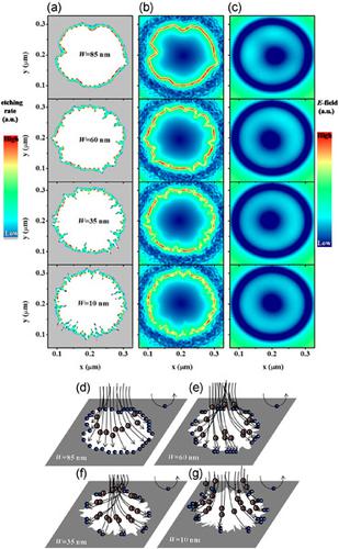
The edge roughness (ER) developed in the mask pattern during the plasma etching process harms the perfect pattern transformation from mask to substrate. To understand and ultimately manipulate plasma‐induced ER, this study investigated the interplay between charging and nanoscale roughness of an isolated rough mask hole in the plasma etching process using a modeling framework, which consisted of a surface etching module, a surface charging module, and a profile evolution module. Specifically, on the one hand, the distributions of the spatial electric field (E‐field) and etching rate were simulated for the rough mask surface being etched. It is revealed that the distribution of the etching rate is similar with that of E‐field clinging to the mask surface, and both of them reach their maximum strength around the mask hole edge and gradually becomes uniform/nonuniform with the decrease of the value of the dominant amplitude/wavelength of roughness; on the other hand, a string algorithm was used to simulate the evolution rule for a rough profile of a mask hole with etching time under various values of roughness parameters. The simulated evolution of the profile has good agreement with experimental observation. The charging effect contributes to the enhancement of the root mean square roughness. Additionally, the influence of roughness parameters on the charging time versus root mean square was also examined. The mechanism behind these results was analyzed systematically. This study will greatly contribute toward improving the physical and chemical properties of the mask or optimizing the etching technique.
中文翻译:

掩模图案的边缘粗糙度与等离子蚀刻中的电荷之间的关系
在等离子蚀刻过程中在掩模图案中形成的边缘粗糙度(ER)会损害从掩模到基板的完美图案转换。为了理解并最终操纵等离子体诱发的ER,本研究使用建模框架研究了等离子体蚀刻过程中孤立的粗糙掩模孔的电荷与纳米级粗糙度之间的相互作用,该模型框架包括表面蚀刻模块,表面充电模块和配置文件演变模块。具体地说,一方面,模拟了被蚀刻的粗糙掩模表面的空间电场(E场)和蚀刻速率的分布。揭示了腐蚀速率的分布与E相似磁场紧贴在掩模表面,并且随着主振幅/粗糙度波长值的减小,它们都在掩模孔边缘附近达到最大强度,并逐渐变得均匀/不均匀;另一方面,在不同的粗糙度参数值下,采用字符串算法模拟了具有刻蚀时间的掩模孔的粗糙轮廓的演变规律。剖面的模拟演变与实验观察有很好的一致性。带电效应有助于提高均方根粗糙度。另外,还检查了粗糙度参数对充电时间对均方根的影响。对这些结果背后的机制进行了系统的分析。
更新日期:2019-11-14
中文翻译:
掩模图案的边缘粗糙度与等离子蚀刻中的电荷之间的关系
在等离子蚀刻过程中在掩模图案中形成的边缘粗糙度(ER)会损害从掩模到基板的完美图案转换。为了理解并最终操纵等离子体诱发的ER,本研究使用建模框架研究了等离子体蚀刻过程中孤立的粗糙掩模孔的电荷与纳米级粗糙度之间的相互作用,该模型框架包括表面蚀刻模块,表面充电模块和配置文件演变模块。具体地说,一方面,模拟了被蚀刻的粗糙掩模表面的空间电场(E场)和蚀刻速率的分布。揭示了腐蚀速率的分布与E相似磁场紧贴在掩模表面,并且随着主振幅/粗糙度波长值的减小,它们都在掩模孔边缘附近达到最大强度,并逐渐变得均匀/不均匀;另一方面,在不同的粗糙度参数值下,采用字符串算法模拟了具有刻蚀时间的掩模孔的粗糙轮廓的演变规律。剖面的模拟演变与实验观察有很好的一致性。带电效应有助于提高均方根粗糙度。另外,还检查了粗糙度参数对充电时间对均方根的影响。对这些结果背后的机制进行了系统的分析。


 京公网安备 11010802027423号