Nature Electronics ( IF 33.7 ) Pub Date : 2019-12-09 , DOI: 10.1038/s41928-019-0338-7 Mengwei Si , Atanu K. Saha , Shengjie Gao , Gang Qiu , Jingkai Qin , Yuqin Duan , Jie Jian , Chang Niu , Haiyan Wang , Wenzhuo Wu , Sumeet K. Gupta , Peide D. Ye
|
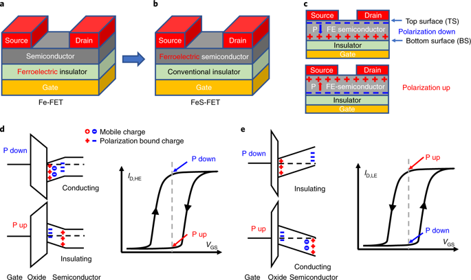
Ferroelectric field-effect transistors employ a ferroelectric material as a gate insulator, the polarization state of which can be detected using the channel conductance of the device. As a result, the devices are potentially of use in non-volatile memory technology, but they suffer from short retention times, which limits their wider application. Here, we report a ferroelectric semiconductor field-effect transistor in which a two-dimensional ferroelectric semiconductor, indium selenide (α-In2Se3), is used as the channel material in the device. α-In2Se3 was chosen due to its appropriate bandgap, room-temperature ferroelectricity, ability to maintain ferroelectricity down to a few atomic layers and its potential for large-area growth. A passivation method based on the atomic layer deposition of aluminium oxide (Al2O3) was developed to protect and enhance the performance of the transistors. With 15-nm-thick hafnium oxide (HfO2) as a scaled gate dielectric, the resulting devices offer high performance with a large memory window, a high on/off ratio of over 108, a maximum on current of 862 μA μm−1 and a low supply voltage.
中文翻译:
铁电半导体场效应晶体管
铁电场效应晶体管采用铁电材料作为栅极绝缘体,可以使用器件的沟道电导来检测其极化状态。结果,这些设备有可能用于非易失性存储技术中,但是它们的保留时间短,这限制了它们的广泛应用。这里,我们报告,其中一个二维铁电体半导体,硒化铟(α-在铁电体半导体场效应晶体管2硒3),被用作该装置中的沟道材料。α-在2硒3选择它的原因是它具有适当的带隙,室温铁电,将铁电保持到几个原子层的能力以及其大面积生长的潜力。为了保护和增强晶体管的性能,开发了一种基于氧化铝(Al 2 O 3)原子层沉积的钝化方法。用15-nm厚的氧化铪(HfO 2),其为经缩放的栅极电介质,所得到的设备提供高性能的具有大存储窗口,通/高离超过10比8,最大电流的862μA微米- 1和低电源电压。


 京公网安备 11010802027423号