当前位置:
X-MOL 学术
›
ACS Photonics
›
论文详情
Our official English website, www.x-mol.net, welcomes your
feedback! (Note: you will need to create a separate account there.)
Stable Efficient Methylammonium Lead Iodide Thin Film Photodetectors with Highly Oriented Millimeter-Sized Crystal Grains
ACS Photonics ( IF 6.5 ) Pub Date : 2019-12-16 , DOI: 10.1021/acsphotonics.9b01455 Md Mehedi Hasan , Charlotte Clegg 1 , Max Manning , Ahmed El Ghanam , Chen Su , Matthew D. Harding , Craig Bennett 2 , Ian G. Hill 1 , Ghada I. Koleilat 1
ACS Photonics ( IF 6.5 ) Pub Date : 2019-12-16 , DOI: 10.1021/acsphotonics.9b01455 Md Mehedi Hasan , Charlotte Clegg 1 , Max Manning , Ahmed El Ghanam , Chen Su , Matthew D. Harding , Craig Bennett 2 , Ian G. Hill 1 , Ghada I. Koleilat 1
Affiliation
|
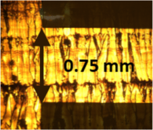
The size of crystal grains in lead halide perovskite thin films remains a vital design feature for durable optoelectronic devices. With larger crystals and reduced grain boundaries per surface area, the stability of the structures improves as degradation, caused by moisture and oxygen percolating into the grain boundaries, is minimized. Thus far, large scale continuous lateral films of methylammonium lead iodide (MAPbI3) with macroscale crystal grains compatible with thin film (<1 μm thick) solar cells and photodetectors have not been reported. Herein, we employ meniscus-guided blade coating technique to grow thin films of highly oriented millimeter-size MAPbI3 crystals, resulting in over an order of magnitude responsivity enhancement over spin-coated films in lateral photoconductors with channel lengths over 100 μm. Furthermore, the blade-coated MAPbI3 thin films exhibit anisotropic higher conductivity along crystal grains over a millimeter range. With crystals orders of magnitude larger in size, and with no additive treatment or additional layers, blade-coated devices manifest improved stability and retain over 80% of their performance tested in ambient air for over 300 h in comparison to spin-coated devices that reach less than 50% of their original peformance within the first 36 h.
中文翻译:

具有高度定向的毫米级晶粒的稳定高效的甲基铵碘化铅薄膜光电探测器
卤化钙钛矿铅薄膜中晶粒的大小对于耐用的光电器件而言仍然是至关重要的设计特征。对于较大的晶体和每表面积减小的晶界,随着水分和氧气渗入晶界引起的降解最小化,结构的稳定性得以改善。迄今为止,尚未报道具有与薄膜太阳能电池和光电检测器兼容的宏观晶粒的大规模连续的甲基碘化碘化铅铅(MAPbI 3)侧面膜。在这里,我们采用弯月面引导刀片涂布技术来生长高度取向的毫米级MAPbI 3薄膜晶体,在通道长度超过100μm的横向光电导体中,其响应度比旋涂膜提高了一个数量级。此外,刮刀涂布的MAPbI 3薄膜沿毫米范围内的晶粒表现出各向异性更高的电导率。与旋转涂覆的装置相比,刀片涂覆的装置具有更大的数量级晶体,并且无需任何附加处理或额外的层,因此具有更高的稳定性,并在环境空气中测试80%以上的性能,可在环境空气中保持300小时以上。在最初的36小时内不到其原始性能的50%。
更新日期:2019-12-17
中文翻译:
具有高度定向的毫米级晶粒的稳定高效的甲基铵碘化铅薄膜光电探测器
卤化钙钛矿铅薄膜中晶粒的大小对于耐用的光电器件而言仍然是至关重要的设计特征。对于较大的晶体和每表面积减小的晶界,随着水分和氧气渗入晶界引起的降解最小化,结构的稳定性得以改善。迄今为止,尚未报道具有与薄膜太阳能电池和光电检测器兼容的宏观晶粒的大规模连续的甲基碘化碘化铅铅(MAPbI 3)侧面膜。在这里,我们采用弯月面引导刀片涂布技术来生长高度取向的毫米级MAPbI 3薄膜晶体,在通道长度超过100μm的横向光电导体中,其响应度比旋涂膜提高了一个数量级。此外,刮刀涂布的MAPbI 3薄膜沿毫米范围内的晶粒表现出各向异性更高的电导率。与旋转涂覆的装置相比,刀片涂覆的装置具有更大的数量级晶体,并且无需任何附加处理或额外的层,因此具有更高的稳定性,并在环境空气中测试80%以上的性能,可在环境空气中保持300小时以上。在最初的36小时内不到其原始性能的50%。


 京公网安备 11010802027423号