当前位置:
X-MOL 学术
›
Prog. Photovoltaics
›
论文详情
Our official English website, www.x-mol.net, welcomes your
feedback! (Note: you will need to create a separate account there.)
Nanosecond laser scribing for see‐through CIGS thin film solar cells
Progress in Photovoltaics ( IF 8.0 ) Pub Date : 2019-12-05 , DOI: 10.1002/pip.3219 Seungkuk Kuk 1 , Zhen Wang 1 , Hyeonggeun Yu 2 , Chang‐Yong Nam 3 , Jeung‐hyun Jeong 2 , David Hwang 1
Progress in Photovoltaics ( IF 8.0 ) Pub Date : 2019-12-05 , DOI: 10.1002/pip.3219 Seungkuk Kuk 1 , Zhen Wang 1 , Hyeonggeun Yu 2 , Chang‐Yong Nam 3 , Jeung‐hyun Jeong 2 , David Hwang 1
Affiliation
|
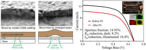
Building‐integrated photovoltaic (BIPV), especially in a semitransparent and/or see‐through configuration, has attracted significant attention because of the extended surfaces available for the photovoltaic (PV) installation including roofs, facades, and windows. In this study, we examine the P4 scribing process for fabricating see‐through cells on a new Cu (In,Ga)Se2 (CIGS) architecture with indium tin oxide (ITO) bottom contact, using a nanosecond laser beam of 532‐nm wavelength illuminated from glass substrate side. Through parametric studies with the variations of laser beam spot size and pulse energy, we have identified that enlarged laser beam with the pulse energy near scribing threshold could suppress both damage in ITO and electrical shunt induced by molten CIGS. Scanning electron microscopy (SEM) and energy‐dispersive X‐ray spectroscopy (EDS) analyses unveil that the molten CIGS mediated shunt mechanism, wetting the scribing edge and forming Cu‐rich metallic phase. The P4 scribing process operated near threshold fluence of enlarged laser beam clearly suppressed unwanted shunt, also minimizing the fluctuation in the desired film removal trend. Thermal analysis supports that enlarged laser beam enables scribing at reduced CIGS‐ITO interface temperature assisted by buckling‐based film delamination mechanism and also suppresses CIGS melting at scribing edge and its neighborhood. See‐through cells fabricated for the areal fraction of approximately 15% using the optimal laser scribing parameters exhibited the short circuit current reduction rate of 16.8% enabled by the low shunt resistance reduction rate of approximately 8%. Further studies are underway to elucidate precise shunt‐related scribing mechanism on the basis of the cross‐sectional analyses and time‐resolved diagnostics and to fabricate the module level see‐through PV architectures.
中文翻译:

纳秒级激光划刻,用于透视CIGS薄膜太阳能电池
建筑集成光伏(BIPV)尤其是半透明和/或透视配置的建筑吸引了广泛的关注,因为可用于光伏(PV)安装的扩展表面包括屋顶,立面和窗户。在这项研究中,我们研究了在新的Cu(In,Ga)Se 2上制造透明电池的P4划片工艺(CIGS)架构具有铟锡氧化物(ITO)底部触点,使用从玻璃基板一侧照射的532 nm波长的纳秒激光束。通过对激光束光斑大小和脉冲能量的变化进行参数研究,我们发现,脉冲能量接近划线阈值的放大激光束既可以抑制ITO的损坏,又可以抑制熔融CIGS引起的电分流。扫描电子显微镜(SEM)和能量色散X射线能谱(EDS)分析表明,熔融的CIGS介导的分流机制,润湿划线边缘并形成富Cu的金属相。P4划片工艺在扩大的激光束的阈值通量附近运行,明显抑制了不必要的分流,也使所需的薄膜去除趋势的波动最小化。热分析表明,借助基于屈曲的薄膜分层机制,扩大的激光束可以在降低的CIGS-ITO界面温度下进行划刻,并且还可以抑制CIGS在划刻边缘及其附近融化。使用最佳激光刻划参数以约15%的面积比例制造的透明电池具有约8%的低分流电阻降低率,实现了16.8%的短路电流降低率。正在进行进一步的研究,以根据横截面分析和时间分辨诊断来阐明与分流器相关的精确划刻机制,并制造模块级透明PV架构。
更新日期:2019-12-05
中文翻译:
纳秒级激光划刻,用于透视CIGS薄膜太阳能电池
建筑集成光伏(BIPV)尤其是半透明和/或透视配置的建筑吸引了广泛的关注,因为可用于光伏(PV)安装的扩展表面包括屋顶,立面和窗户。在这项研究中,我们研究了在新的Cu(In,Ga)Se 2上制造透明电池的P4划片工艺(CIGS)架构具有铟锡氧化物(ITO)底部触点,使用从玻璃基板一侧照射的532 nm波长的纳秒激光束。通过对激光束光斑大小和脉冲能量的变化进行参数研究,我们发现,脉冲能量接近划线阈值的放大激光束既可以抑制ITO的损坏,又可以抑制熔融CIGS引起的电分流。扫描电子显微镜(SEM)和能量色散X射线能谱(EDS)分析表明,熔融的CIGS介导的分流机制,润湿划线边缘并形成富Cu的金属相。P4划片工艺在扩大的激光束的阈值通量附近运行,明显抑制了不必要的分流,也使所需的薄膜去除趋势的波动最小化。热分析表明,借助基于屈曲的薄膜分层机制,扩大的激光束可以在降低的CIGS-ITO界面温度下进行划刻,并且还可以抑制CIGS在划刻边缘及其附近融化。使用最佳激光刻划参数以约15%的面积比例制造的透明电池具有约8%的低分流电阻降低率,实现了16.8%的短路电流降低率。正在进行进一步的研究,以根据横截面分析和时间分辨诊断来阐明与分流器相关的精确划刻机制,并制造模块级透明PV架构。


 京公网安备 11010802027423号