Microsystems & Nanoengineering ( IF 7.3 ) Pub Date : 2019-12-02 , DOI: 10.1038/s41378-019-0101-2 Pierre-Marie Coulon 1 , Benjamin Damilano 2 , Blandine Alloing 2 , Pierre Chausse 1 , Sebastian Walde 3 , Johannes Enslin 4 , Robert Armstrong 1 , Stéphane Vézian 2 , Sylvia Hagedorn 3 , Tim Wernicke 4 , Jean Massies 2 , Jesus Zúñiga-Pérez 2 , Markus Weyers 3 , Michael Kneissl 3, 4 , Philip A Shields 1
|
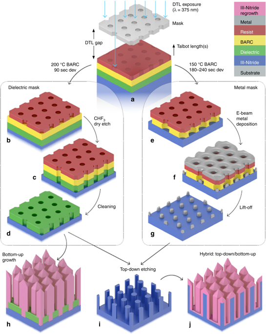
Nano-engineering III-nitride semiconductors offers a route to further control the optoelectronic properties, enabling novel functionalities and applications. Although a variety of lithography techniques are currently employed to nano-engineer these materials, the scalability and cost of the fabrication process can be an obstacle for large-scale manufacturing. In this paper, we report on the use of a fast, robust and flexible emerging patterning technique called Displacement Talbot lithography (DTL), to successfully nano-engineer III-nitride materials. DTL, along with its novel and unique combination with a lateral planar displacement (D2TL), allow the fabrication of a variety of periodic nanopatterns with a broad range of filling factors such as nanoholes, nanodots, nanorings and nanolines; all these features being achievable from one single mask. To illustrate the enormous possibilities opened by DTL/D2TL, dielectric and metal masks with a number of nanopatterns have been generated, allowing for the selective area growth of InGaN/GaN core-shell nanorods, the top-down plasma etching of III-nitride nanostructures, the top-down sublimation of GaN nanostructures, the hybrid top-down/bottom-up growth of AlN nanorods and GaN nanotubes, and the fabrication of nanopatterned sapphire substrates for AlN growth. Compared with their planar counterparts, these 3D nanostructures enable the reduction or filtering of structural defects and/or the enhancement of the light extraction, therefore improving the efficiency of the final device. These results, achieved on a wafer scale via DTL and upscalable to larger surfaces, have the potential to unlock the manufacturing of nano-engineered III-nitride materials.
中文翻译:
用于 III 族氮化物材料纳米工程的位移 Talbot 光刻
纳米工程 III 族氮化物半导体提供了进一步控制光电特性的途径,从而实现了新的功能和应用。尽管目前采用各种光刻技术对这些材料进行纳米工程,但制造过程的可扩展性和成本可能成为大规模制造的障碍。在本文中,我们报告了使用称为位移 Talbot 光刻 (DTL) 的快速、稳健和灵活的新兴图案化技术,成功地纳米工程 III 族氮化物材料。DTL,连同其新颖独特的横向平面位移组合 (D 2TL),允许制造具有广泛填充因子的各种周期性纳米图案,例如纳米孔、纳米点、纳米环和纳米线;所有这些功能都可以通过一个面罩实现。说明 DTL/D 2打开的巨大可能性已生成具有多个纳米图案的 TL、电介质和金属掩模,允许 InGaN/GaN 核壳纳米棒的选择性区域生长、III 族氮化物纳米结构的自上而下等离子体蚀刻、GaN 纳米结构的自上而下升华,AlN 纳米棒和 GaN 纳米管的自上而下/自下而上的混合生长,以及用于 AlN 生长的纳米图案蓝宝石衬底的制造。与其平面对应物相比,这些 3D 纳米结构能够减少或过滤结构缺陷和/或增强光提取,从而提高最终设备的效率。这些结果是通过 DTL 在晶圆规模上实现的,并且可以放大到更大的表面,有可能开启纳米工程 III 族氮化物材料的制造。


 京公网安备 11010802027423号