当前位置:
X-MOL 学术
›
Adv. Electron. Mater.
›
论文详情
Our official English website, www.x-mol.net, welcomes your
feedback! (Note: you will need to create a separate account there.)
High‐Performance Polycrystalline Silicon Thin‐Film Transistors without Source/Drain Doping by Utilizing Anisotropic Conductivity of Bridged‐Grain Lines
Advanced Electronic Materials ( IF 5.3 ) Pub Date : 2019-12-01 , DOI: 10.1002/aelm.201900961 Meng Zhang 1 , Haotao Lin 1 , Sunbin Deng 2 , Rongsheng Chen 3 , Guijun Li 4 , Su‐Ting Han 1 , Ye Zhou 5 , Yan Yan 1 , Wei Zhou 6 , Man Wong 2 , Hoi‐Sing Kwok 2
Advanced Electronic Materials ( IF 5.3 ) Pub Date : 2019-12-01 , DOI: 10.1002/aelm.201900961 Meng Zhang 1 , Haotao Lin 1 , Sunbin Deng 2 , Rongsheng Chen 3 , Guijun Li 4 , Su‐Ting Han 1 , Ye Zhou 5 , Yan Yan 1 , Wei Zhou 6 , Man Wong 2 , Hoi‐Sing Kwok 2
Affiliation
|
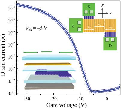
By utilizing anisotropic conductivity of bridged‐grain (BG) lines, a polycrystalline silicon (poly‐Si) thin‐film transistor (TFT) without source/drain (S/D) doping is designed, simulated, and fabricated. In the new design, the current is made to flow along the BG lines in the S/D region and flow perpendicularly to the BG lines in the channel. By taking advantage of the anisotropic conductivity of the BG lines, the S/D doping process is eliminated and the fabrication process cost is reduced. Meanwhile, the advantages of adopting BG lines are maintained. The as‐fabricated TFTs without S/D doping exhibit excellent device characteristics, compared with normal TFTs. The reliability of TFTs without S/D doping is also evaluated under hot carrier stress and negative/positive bias stress. Additionally, the proposed new TFT structure allows a wider range of dopant activation conditions.
中文翻译:

利用桥式晶粒线的各向异性电导率而无需源极/漏极掺杂的高性能多晶硅薄膜晶体管
通过利用桥接晶粒(BG)线的各向异性电导率,设计,模拟和制造了无源极/漏极(S / D)掺杂的多晶硅(poly-Si)薄膜晶体管(TFT)。在新设计中,使电流沿S / D区域中的BG线流动,并垂直于通道中的BG线流动。通过利用BG线的各向异性导电性,消除了S / D掺杂工艺,并降低了制造工艺成本。同时,保持了采用BG生产线的优势。与普通TFT相比,没有S / D掺杂的预制TFT表现出优异的器件特性。还可以在热载流子应力和负/正偏应力下评估没有S / D掺杂的TFT的可靠性。此外,
更新日期:2020-02-13
中文翻译:
利用桥式晶粒线的各向异性电导率而无需源极/漏极掺杂的高性能多晶硅薄膜晶体管
通过利用桥接晶粒(BG)线的各向异性电导率,设计,模拟和制造了无源极/漏极(S / D)掺杂的多晶硅(poly-Si)薄膜晶体管(TFT)。在新设计中,使电流沿S / D区域中的BG线流动,并垂直于通道中的BG线流动。通过利用BG线的各向异性导电性,消除了S / D掺杂工艺,并降低了制造工艺成本。同时,保持了采用BG生产线的优势。与普通TFT相比,没有S / D掺杂的预制TFT表现出优异的器件特性。还可以在热载流子应力和负/正偏应力下评估没有S / D掺杂的TFT的可靠性。此外,


 京公网安备 11010802027423号