Our official English website, www.x-mol.net, welcomes your
feedback! (Note: you will need to create a separate account there.)
Continuous-wave electrically pumped 1550 nm lasers epitaxially grown on on-axis (001) silicon
Optica ( IF 8.4 ) Pub Date : 2019-12-03 , DOI: 10.1364/optica.6.001507 Bei Shi , Hongwei Zhao , Lei Wang , Bowen Song , Simone Tommaso Suran Brunelli , Jonathan Klamkin
Optica ( IF 8.4 ) Pub Date : 2019-12-03 , DOI: 10.1364/optica.6.001507 Bei Shi , Hongwei Zhao , Lei Wang , Bowen Song , Simone Tommaso Suran Brunelli , Jonathan Klamkin
|
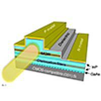
Heteroepitaxy of III–V compound semiconductors on industry standard (001) silicon (Si) substrates is highly desirable for large-scale electronic and photonic integrated circuits. Challenges of this approach relate primarily to lattice, polarity, and coefficient of thermal expansion mismatch, which ultimately generate a high density of defects and limit the reliability of active devices. Ongoing efforts to monolithically integrate lasers in silicon photonics include leveraging quantum dots for reduced sensitivity to defects and the ability to enable 1310 nm lasers with gallium arsenide (GaAs) and related compounds. In this work, to extend the operation window to the widely used 1550 nm telecommunications region, we have demonstrated continuous-wave (CW) electrically pumped indium phosphide (InP)-based quantum well lasers on complementary metal-oxide-semiconductor (CMOS)-compatible (001) Si. Heteroepitaxy of InP and related compounds on Si poses additional challenges because the lattice mismatch is significantly larger compared to GaAs. Key to our approach is the development of a low dislocation density InP-on-Si template by metalorganic chemical vapor deposition (MOCVD). Following an InP buffer with a surface defect density of ${1.15} \times {{10}^8}/{{\rm cm}^2}$, a seven-layer indium gallium arsenide phosphide (InGaAsP) multi-quantum well laser diode structure was grown. Fabry–Perot ridge waveguide lasers were then fabricated. A 20-µm wide and 1000-µm long laser demonstrates a room temperature continuous-wave (CW) lasing threshold current density of ${2.05}\;{{\rm kA}/{\rm cm}^2}$ and a maximum output power of 18 mW per facet without facet coating. CW lasing up to 65°C and pulsed lasing greater than 105°C were achieved. This MOCVD-based heteroepitaxy approach offers a practical path toward monolithic integration of InP lasers in silicon photonics.
中文翻译:

在同轴(001)硅上外延生长的连续波电泵浦1550 nm激光器
对于大型电子和光子集成电路,行业标准(001)硅(Si)衬底上的III–V类化合物半导体的异质外延非常理想。这种方法的挑战主要与晶格,极性和热膨胀系数不匹配有关,这最终会产生高密度的缺陷并限制有源器件的可靠性。将激光器单片集成到硅光子中的正在进行的工作包括利用量子点降低对缺陷的敏感性,并能够使用砷化镓(GaAs)和相关化合物来实现1310 nm激光器。在这项工作中,为了将操作窗口扩展到广泛使用的1550 nm电信区域,我们已经证明了在互补金属氧化物半导体(CMOS)兼容(001)硅上的连续波(CW)电泵浦磷化铟(InP)基量子阱激光器。InP和相关化合物在Si上的异质外延构成了其他挑战,因为与GaAs相比,晶格失配明显更大。我们方法的关键是通过金属有机化学气相沉积(MOCVD)开发低位错密度的InP-on-Si模板。跟随表面缺陷密度为InP的InP缓冲液$ {1.15} \ {{10} ^ 8} / {{\ rm cm} ^ 2} $,生长了七层砷化铟镓磷化物(InGaAsP)多量子阱激光二极管结构。然后制造了法布里-珀罗脊形波导激光器。一个20 µm宽且1000 µm长的激光器显示出室温连续波(CW)激射阈值电流密度为$ {2.05} \; {{\ rm kA} / {\ rm cm} ^ 2} $和一个无刻面涂层时,每刻面的最大输出功率为18 mW。实现了高达65°C的CW激光和大于105°C的脉冲激光。这种基于MOCVD的异质外延方法为InP激光器在硅光子学中的单片集成提供了一条实用的途径。
更新日期:2019-12-21
中文翻译:
在同轴(001)硅上外延生长的连续波电泵浦1550 nm激光器
对于大型电子和光子集成电路,行业标准(001)硅(Si)衬底上的III–V类化合物半导体的异质外延非常理想。这种方法的挑战主要与晶格,极性和热膨胀系数不匹配有关,这最终会产生高密度的缺陷并限制有源器件的可靠性。将激光器单片集成到硅光子中的正在进行的工作包括利用量子点降低对缺陷的敏感性,并能够使用砷化镓(GaAs)和相关化合物来实现1310 nm激光器。在这项工作中,为了将操作窗口扩展到广泛使用的1550 nm电信区域,我们已经证明了在互补金属氧化物半导体(CMOS)兼容(001)硅上的连续波(CW)电泵浦磷化铟(InP)基量子阱激光器。InP和相关化合物在Si上的异质外延构成了其他挑战,因为与GaAs相比,晶格失配明显更大。我们方法的关键是通过金属有机化学气相沉积(MOCVD)开发低位错密度的InP-on-Si模板。跟随表面缺陷密度为InP的InP缓冲液$ {1.15} \ {{10} ^ 8} / {{\ rm cm} ^ 2} $,生长了七层砷化铟镓磷化物(InGaAsP)多量子阱激光二极管结构。然后制造了法布里-珀罗脊形波导激光器。一个20 µm宽且1000 µm长的激光器显示出室温连续波(CW)激射阈值电流密度为$ {2.05} \; {{\ rm kA} / {\ rm cm} ^ 2} $和一个无刻面涂层时,每刻面的最大输出功率为18 mW。实现了高达65°C的CW激光和大于105°C的脉冲激光。这种基于MOCVD的异质外延方法为InP激光器在硅光子学中的单片集成提供了一条实用的途径。


 京公网安备 11010802027423号