Our official English website, www.x-mol.net, welcomes your
feedback! (Note: you will need to create a separate account there.)
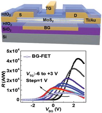
A Dual-Gate MoS2 Photodetector Based on Interface Coupling Effect.
Small ( IF 13.0 ) Pub Date : 2019-11-26 , DOI: 10.1002/smll.201904369 Fuyou Liao 1 , Jianan Deng 2 , Xinyu Chen 1 , Yin Wang 1 , Xinzhi Zhang 1 , Jian Liu 2 , Hao Zhu 1 , Lin Chen 1 , Qingqing Sun 1 , Weida Hu 3 , Jianlu Wang 3 , Jing Zhou 3 , Peng Zhou 1 , David Wei Zhang 1 , Jing Wan 2 , Wenzhong Bao 1
Small ( IF 13.0 ) Pub Date : 2019-11-26 , DOI: 10.1002/smll.201904369 Fuyou Liao 1 , Jianan Deng 2 , Xinyu Chen 1 , Yin Wang 1 , Xinzhi Zhang 1 , Jian Liu 2 , Hao Zhu 1 , Lin Chen 1 , Qingqing Sun 1 , Weida Hu 3 , Jianlu Wang 3 , Jing Zhou 3 , Peng Zhou 1 , David Wei Zhang 1 , Jing Wan 2 , Wenzhong Bao 1
Affiliation
|
2D transition metal dichalcogenides (TMDs) based photodetectors have shown great potential for the next generation optoelectronics. However, most of the reported MoS2 photodetectors function under the photogating effect originated from the charge-trap mechanism, which is difficult for quantitative control. Such devices generally suffer from a poor compromise between response speed and responsivity (R) and large dark current. Here, a dual-gated (DG) MoS2 phototransistor operating based on the interface coupling effect (ICE) is demonstrated. By simultaneously applying a negative top-gate voltage (VTG ) and positive back-gate voltage (VBG ) to the MoS2 channel, the photogenerated holes can be effectively trapped in the depleted region under TG. An ultrahigh R of ≈105 A W-1 and detectivity (D*) of ≈1014 Jones are achieved in several devices with different thickness under Pin of 53 µW cm-2 at VTG = -5 V. Moreover, the response time of the DG phototransistor can also be modulated based on the ICE. Based on these systematic measurements of MoS2 DG phototransistors, the results show that the ICE plays an important role in the modulation of photoelectric performances. The results also pave the way for the future optoelectrical application of 2D TMDs materials and prompt for further investigation in the DG structured phototransistors.
中文翻译:

基于界面耦合效应的双栅极MoS2光电探测器。
基于2D过渡金属二硫化碳(TMD)的光电检测器已显示出下一代光电技术的巨大潜力。然而,大多数报道的MoS2光电探测器在光门作用下起着电荷捕获机制的作用,这很难进行定量控制。这样的设备通常遭受响应速度和响应度(R)之间的差的折衷以及大的暗电流。在此,说明了基于界面耦合效应(ICE)的双栅极(DG)MoS2光电晶体管。通过同时向MoS2通道施加负的顶栅电压(VTG)和正的背栅电压(VBG),可以将光生空穴有效地捕获在TG之下的耗尽区中。在VTG = -5 V时,在引脚厚度为53 µW cm-2的情况下,采用不同厚度的几种器件,可以实现≈105A W-1的超高R-1和≈1014Jones的检测灵敏度(D *)。 DG光电晶体管也可以基于ICE进行调制。基于对MoS2 DG光电晶体管的这些系统测量,结果表明ICE在光电性能的调制中起着重要作用。这些结果也为将来2D TMDs材料的光电应用铺平了道路,并为在DG结构的光电晶体管中进行进一步的研究提供了提示。结果表明,ICE在光电性能的调节中起着重要作用。这些结果也为未来2D TMDs材料的光电应用铺平了道路,并为在DG结构的光电晶体管中进行进一步的研究提供了提示。结果表明,ICE在光电性能的调节中起着重要作用。这些结果也为未来2D TMDs材料的光电应用铺平了道路,并为在DG结构的光电晶体管中进行进一步的研究提供了提示。
更新日期:2020-01-09
中文翻译:
基于界面耦合效应的双栅极MoS2光电探测器。
基于2D过渡金属二硫化碳(TMD)的光电检测器已显示出下一代光电技术的巨大潜力。然而,大多数报道的MoS2光电探测器在光门作用下起着电荷捕获机制的作用,这很难进行定量控制。这样的设备通常遭受响应速度和响应度(R)之间的差的折衷以及大的暗电流。在此,说明了基于界面耦合效应(ICE)的双栅极(DG)MoS2光电晶体管。通过同时向MoS2通道施加负的顶栅电压(VTG)和正的背栅电压(VBG),可以将光生空穴有效地捕获在TG之下的耗尽区中。在VTG = -5 V时,在引脚厚度为53 µW cm-2的情况下,采用不同厚度的几种器件,可以实现≈105A W-1的超高R-1和≈1014Jones的检测灵敏度(D *)。 DG光电晶体管也可以基于ICE进行调制。基于对MoS2 DG光电晶体管的这些系统测量,结果表明ICE在光电性能的调制中起着重要作用。这些结果也为将来2D TMDs材料的光电应用铺平了道路,并为在DG结构的光电晶体管中进行进一步的研究提供了提示。结果表明,ICE在光电性能的调节中起着重要作用。这些结果也为未来2D TMDs材料的光电应用铺平了道路,并为在DG结构的光电晶体管中进行进一步的研究提供了提示。结果表明,ICE在光电性能的调节中起着重要作用。这些结果也为未来2D TMDs材料的光电应用铺平了道路,并为在DG结构的光电晶体管中进行进一步的研究提供了提示。


 京公网安备 11010802027423号