当前位置:
X-MOL 学术
›
Adv. Electron. Mater.
›
论文详情
Our official English website, www.x-mol.net, welcomes your
feedback! (Note: you will need to create a separate account there.)
Polymer Light‐Emitting Transistors With Charge‐Carrier Mobilities Exceeding 1 cm2 V−1 s−1
Advanced Electronic Materials ( IF 5.3 ) Pub Date : 2019-11-25 , DOI: 10.1002/aelm.201901132 Mujeeb Ullah Chaudhry 1 , Julianna Panidi 2 , Sungho Nam 3 , Alice Smith 3 , Jongchul Lim 3 , Kornelius Tetzner 2 , Panos A. Patsalas 4 , George Vourlias 4 , Wai‐Yu Sit 2 , Yuliar Firdaus 5 , Martin Heeney 6 , Donal D. C. Bradley 3, 5, 7 , Thomas D. Anthopoulos 2, 5
Advanced Electronic Materials ( IF 5.3 ) Pub Date : 2019-11-25 , DOI: 10.1002/aelm.201901132 Mujeeb Ullah Chaudhry 1 , Julianna Panidi 2 , Sungho Nam 3 , Alice Smith 3 , Jongchul Lim 3 , Kornelius Tetzner 2 , Panos A. Patsalas 4 , George Vourlias 4 , Wai‐Yu Sit 2 , Yuliar Firdaus 5 , Martin Heeney 6 , Donal D. C. Bradley 3, 5, 7 , Thomas D. Anthopoulos 2, 5
Affiliation
|
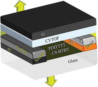
The vast majority of conjugated‐polymer‐based light emitting field‐effect transistors (LEFETs) are characterized by low charge‐carrier mobilities typically in the 10−5 to 10−3 cm2 V−1 s−1 range. Fast carrier transport is a highly desirable characteristic for high‐frequency LEFET operation and, potentially, for use in electrically pumped lasers. Unfortunately, high‐mobility organic semiconductors are often characterized by strong intermolecular π–π interactions that reduce luminescence. Development of new materials and/or device concepts that overcome this hurdle are therefore required. Single organic semiconductor layer based LEFETs that combine high hole mobilities with encouraging light emission characteristics are reported. This is achieved in a single polymer layer LEFET, which is further enhanced through the use of a small‐molecule/conjugated polymer blend system that possesses a film microstructure which supports enhanced charge‐carrier mobility (3.2 cm2 V−1 s−1) and promising light‐emission characteristics (1600 cd m−2) as compared to polymer‐only based LEFETs. This simple approach represents an attractive strategy to further advance the performance of solution‐processed LEFETs.
中文翻译:

电荷载流子超过1 cm2 V-1 s-1的聚合物发光晶体管
绝大多数基于共轭聚合物的发光场效应晶体管(LEFET)的特点是载流子迁移率低,通常在10 -5至10 -3 cm 2 V -1 s -1范围。快速载流子传输是高频LEFET操作非常需要的特性,并且有可能用于电泵浦激光器。不幸的是,高迁移率的有机半导体通常具有强烈的分子间π-π相互作用,从而减少了发光。因此,需要开发克服该障碍的新材料和/或装置概念。据报道,基于单有机半导体层的LEFET结合了高空穴迁移率和令人鼓舞的发光特性。这是在单个聚合物层LEFET中实现的,可通过使用具有膜微结构的小分子/共轭聚合物共混体系进一步增强该结构,从而支持增强的电荷载流子迁移率(3.2 cm 2 V -1 s-1)和有希望的发光特性(1600 cd m -2),与仅基于聚合物的LEFET相比。这种简单的方法代表了一种诱人的策略,可以进一步提高解决方案处理的LEFET的性能。
更新日期:2020-01-13
中文翻译:
电荷载流子超过1 cm2 V-1 s-1的聚合物发光晶体管
绝大多数基于共轭聚合物的发光场效应晶体管(LEFET)的特点是载流子迁移率低,通常在10 -5至10 -3 cm 2 V -1 s -1范围。快速载流子传输是高频LEFET操作非常需要的特性,并且有可能用于电泵浦激光器。不幸的是,高迁移率的有机半导体通常具有强烈的分子间π-π相互作用,从而减少了发光。因此,需要开发克服该障碍的新材料和/或装置概念。据报道,基于单有机半导体层的LEFET结合了高空穴迁移率和令人鼓舞的发光特性。这是在单个聚合物层LEFET中实现的,可通过使用具有膜微结构的小分子/共轭聚合物共混体系进一步增强该结构,从而支持增强的电荷载流子迁移率(3.2 cm 2 V -1 s-1)和有希望的发光特性(1600 cd m -2),与仅基于聚合物的LEFET相比。这种简单的方法代表了一种诱人的策略,可以进一步提高解决方案处理的LEFET的性能。


 京公网安备 11010802027423号