npj Quantum Information ( IF 6.6 ) Pub Date : 2019-11-22 , DOI: 10.1038/s41534-019-0224-1 Jürgen Lisenfeld , Alexander Bilmes , Anthony Megrant , Rami Barends , Julian Kelly , Paul Klimov , Georg Weiss , John M. Martinis , Alexey V. Ustinov
|
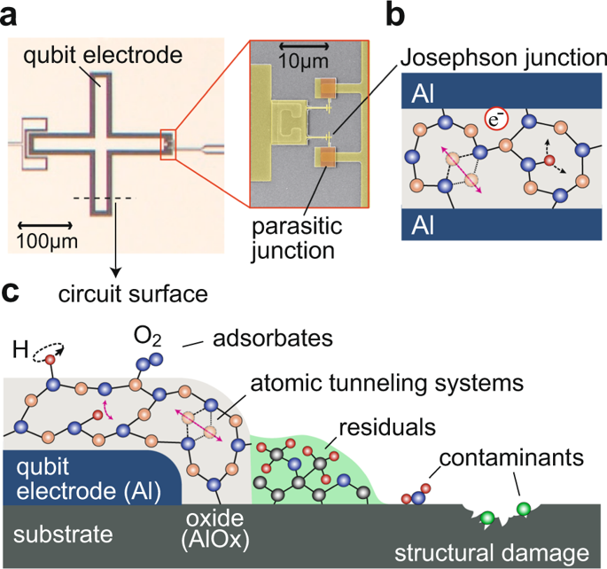
Superconducting integrated circuits have demonstrated a tremendous potential to realize integrated quantum computing processors. However, the downside of the solid-state approach is that superconducting qubits suffer strongly from energy dissipation and environmental fluctuations caused by atomic-scale defects in device materials. Further progress towards upscaled quantum processors will require improvements in device fabrication techniques, which need to be guided by novel analysis methods to understand and prevent mechanisms of defect formation. Here, we present a technique to analyse individual defects in superconducting qubits by tuning them with applied electric fields. This provides a spectroscopy method to extract the defects’ energy distribution, electric dipole moments, and coherence times. Moreover, it enables one to distinguish defects residing in Josephson junction tunnel barriers from those at circuit interfaces. We find that defects at circuit interfaces are responsible for about 60% of the dielectric loss in the investigated transmon qubit sample. About 40% of all detected defects are contained in the tunnel barriers of the large-area parasitic Josephson junctions that occur collaterally in shadow evaporation, and only \(\approx\)3% are identified as strongly coupled defects, which presumably reside in the small-area qubit tunnel junctions. The demonstrated technique provides a valuable tool to assess the decoherence sources related to circuit interfaces and to tunnel junctions that is readily applicable to standard qubit samples.
中文翻译:
跨量子比特中材料缺陷的电场光谱
超导集成电路已经显示出实现集成量子计算处理器的巨大潜力。但是,固态方法的缺点是,超导量子位受器件材料中原子级缺陷引起的能量耗散和环境波动的影响很大。向高级量子处理器的进一步进步将需要器件制造技术的改进,这需要以新颖的分析方法为指导,以理解和防止缺陷形成的机理。在这里,我们提出一种通过对超导量子位中的单个缺陷进行外加电场分析来分析其缺陷的技术。这提供了一种光谱方法来提取缺陷的能量分布,电偶极矩和相干时间。而且,它使人们能够将约瑟夫森结隧道势垒中的缺陷与电路接口处的缺陷区分开。我们发现,在电路接口缺陷中,约60%的跨载量子比特样品的介电损耗是造成的。所有检测到的缺陷中约有40%包含在大面积寄生约瑟夫森结的隧道势垒中,这些势垒在阴影蒸发中并行发生,并且只有\(\约\) 3%被鉴定为强耦合的缺陷,这大概驻留在小面积量子位隧道结。所展示的技术提供了一种有价值的工具,可用来评估与电路接口和隧道结相关的退相干源,该干裂源易于应用于标准量子比特样本。


 京公网安备 11010802027423号