Materials Science and Engineering: B ( IF 3.9 ) Pub Date : 2019-11-09 , DOI: 10.1016/j.mseb.2019.114445 Sibel Gürakar , Tülay Serin
|
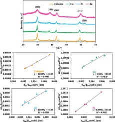
The undoped, Cu, Al and In (2 at. %) doped SnO2 thin films are deposited on the glass substrate by spray pyrolysis. The effect of Cu, Al and In doping on the structural properties of SnO2 films are investigated by X-ray diffraction (XRD) method. All structural parameters including crystallite size, lattice strain, stress and energy density values are determined from three different models based on Williamson-Hall (W-H) and size-strain plot (SSP) methods. The obtained results reveal that strain values are almost the same but crystallite size, stress and energy density values of the films are greatly affected by dopant atoms. Surface morphologies are analyzed using atomic force microscopy (AFM) measurements. The electrical properties are investigated by Hall effect measurements at room temperature. The number of valance electrons of dopant atoms are less than Sn, as a result the decrement in electrical conductivity and the compensation of n-type conductivity are observed.
中文翻译:
(Cu,Al和In)掺杂SnO 2薄膜的综合结构分析和电性能
通过喷雾热解将未掺杂的Cu,Al和In(2原子%)掺杂的SnO 2薄膜沉积在玻璃基板上。Cu,Al和In掺杂对SnO 2结构性能的影响通过X射线衍射(XRD)方法研究薄膜。所有结构参数,包括微晶尺寸,晶格应变,应力和能量密度值,都是根据Williamson-Hall(WH)和尺寸应变图(SSP)方法从三个不同的模型确定的。获得的结果表明,应变值几乎相同,但是薄膜的微晶尺寸,应力和能量密度值受掺杂原子的影响很大。使用原子力显微镜(AFM)测量分析表面形态。通过在室温下的霍尔效应测量来研究电性能。掺杂原子的价电子数小于Sn,结果观察到电导率的下降和n型电导率的补偿。


 京公网安备 11010802027423号