当前位置:
X-MOL 学术
›
Adv. Opt. Mater.
›
论文详情
Our official English website, www.x-mol.net, welcomes your
feedback! (Note: you will need to create a separate account there.)
Efficient All‐Solution‐Processed Perovskite Light‐Emitting Diodes Enabled by Small‐Molecule Doped Electron Injection Layers
Advanced Optical Materials ( IF 8.0 ) Pub Date : 2019-11-07 , DOI: 10.1002/adom.201900567 Jianfeng Zhang 1 , Haoran Wang 1 , Fan Cao 1 , Sheng Wang 1 , Jialong Wu 1 , Yongjiang Dou 1 , Jianhua Zhang 1 , Jing Chen 2 , Dewei Zhao 3, 4 , Xuyong Yang 1
Advanced Optical Materials ( IF 8.0 ) Pub Date : 2019-11-07 , DOI: 10.1002/adom.201900567 Jianfeng Zhang 1 , Haoran Wang 1 , Fan Cao 1 , Sheng Wang 1 , Jialong Wu 1 , Yongjiang Dou 1 , Jianhua Zhang 1 , Jing Chen 2 , Dewei Zhao 3, 4 , Xuyong Yang 1
Affiliation
|
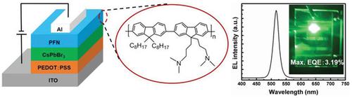
Metal halide perovskites have attracted considerable attention in the field of light‐emitting diodes due to their high color purity and solution processability. However, most perovskite light‐emitting diodes (PeLEDs) employ thermally deposited charge transport layers (CTLs) on top of perovskite layers. In order to realize low‐cost and scalable fabrication of PeLEDs, all‐solution process is highly desired, but still remaining great challenges. Here, an efficient all‐solution‐processed green PeLEDs is reported by incorporating 1,3,5‐tris(1‐phenyl‐1H‐benzimidazol‐2‐yl)benzene (TPBi) doped conjugated amino‐alkyl substituted polyfluorene poly[(9,9‐bis(3′‐(N,N‐dimethylamino)propyl)‐2,7‐fluorene)‐alt‐2,7‐(9,9‐dioctylfluorene)] (PFN) electron injection layer, achieving a maximum luminance of 9875 cd m−2, a high current efficiency of 10.41 cd A−1, and an external quantum efficiency of 3.19%. Since the solvents used for perovskite precursors and PFN are orthogonal, the protected and complete interface of perovskite film and CTL is effectively obtained by solution processes. The doping of TPBi into PFN not only enhances the capability of electron injection, but also significantly suppresses the emission quenching of perovskite films caused by the charge transfer between perovskite and PFN due to the reduced difference in their work functions. This work provides an efficient approach for the development of all‐solution‐processed PeLEDs.
中文翻译:

小分子掺杂电子注入层实现的高效全溶液加工钙钛矿发光二极管
金属卤化物钙钛矿因其高色纯度和溶液加工性而在发光二极管领域引起了相当大的关注。但是,大多数钙钛矿发光二极管(PeLED)在钙钛矿层的顶部均采用热沉积电荷传输层(CTL)。为了实现PeLED的低成本和可扩展制造,人们非常希望采用全解决方案,但仍然面临着巨大的挑战。在这里,通过掺入1,3,5-三(1-苯基-1H-苯并咪唑-2-基)苯(TPBi)掺杂的共轭氨基-烷基取代的聚芴聚[[9 ,9‐双(3'‐(N,N‐二甲基氨基)丙基)‐2,7‐芴)‐alt-2,7-(9,9-二辛基芴)](PFN)电子注入层,可实现9875 cd m -2的最大亮度,10.41 cd A -1的高电流效率和3.19%的外部量子效率。由于用于钙钛矿前体和PFN的溶剂是正交的,因此可以通过溶液法有效地获得钙钛矿膜和CTL的保护和完整界面。将TPBi掺杂到PFN中,不仅增强了电子注入的能力,而且由于钙钛矿与PFN之间的功函数差异减小,钙钛矿膜因电荷转移而引起的钙钛矿薄膜的发射猝灭也得到了抑制。这项工作为开发全解决方案的PeLED提供了一种有效的方法。
更新日期:2020-01-17
中文翻译:
小分子掺杂电子注入层实现的高效全溶液加工钙钛矿发光二极管
金属卤化物钙钛矿因其高色纯度和溶液加工性而在发光二极管领域引起了相当大的关注。但是,大多数钙钛矿发光二极管(PeLED)在钙钛矿层的顶部均采用热沉积电荷传输层(CTL)。为了实现PeLED的低成本和可扩展制造,人们非常希望采用全解决方案,但仍然面临着巨大的挑战。在这里,通过掺入1,3,5-三(1-苯基-1H-苯并咪唑-2-基)苯(TPBi)掺杂的共轭氨基-烷基取代的聚芴聚[[9 ,9‐双(3'‐(N,N‐二甲基氨基)丙基)‐2,7‐芴)‐alt-2,7-(9,9-二辛基芴)](PFN)电子注入层,可实现9875 cd m -2的最大亮度,10.41 cd A -1的高电流效率和3.19%的外部量子效率。由于用于钙钛矿前体和PFN的溶剂是正交的,因此可以通过溶液法有效地获得钙钛矿膜和CTL的保护和完整界面。将TPBi掺杂到PFN中,不仅增强了电子注入的能力,而且由于钙钛矿与PFN之间的功函数差异减小,钙钛矿膜因电荷转移而引起的钙钛矿薄膜的发射猝灭也得到了抑制。这项工作为开发全解决方案的PeLED提供了一种有效的方法。


 京公网安备 11010802027423号