当前位置:
X-MOL 学术
›
Cryst. Res. Technol.
›
论文详情
Our official English website, www.x-mol.net, welcomes your
feedback! (Note: you will need to create a separate account there.)
Growth and Properties of Intentionally Carbon‐Doped GaN Layers
Crystal Research and Technology ( IF 1.5 ) Pub Date : 2019-10-22 , DOI: 10.1002/crat.201900129 Eberhard Richter 1 , Franziska C. Beyer 2 , Friederike Zimmermann 2 , Günter Gärtner 3 , Klaus Irmscher 4 , Ivan Gamov 4 , Johannes Heitmann 2 , Markus Weyers 1 , Günther Tränkle 1
Crystal Research and Technology ( IF 1.5 ) Pub Date : 2019-10-22 , DOI: 10.1002/crat.201900129 Eberhard Richter 1 , Franziska C. Beyer 2 , Friederike Zimmermann 2 , Günter Gärtner 3 , Klaus Irmscher 4 , Ivan Gamov 4 , Johannes Heitmann 2 , Markus Weyers 1 , Günther Tränkle 1
Affiliation
|
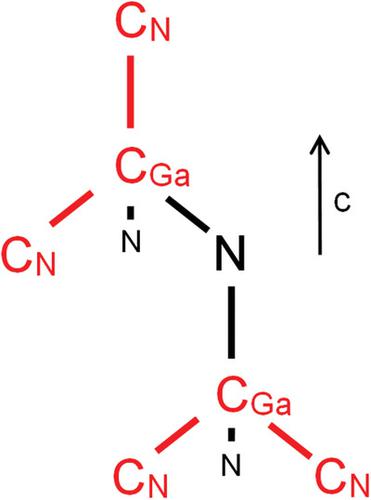
Carbon‐doping of GaN layers with thickness in the mm‐range is performed by hydride vapor phase epitaxy. Characterization by optical and electrical measurements reveals semi‐insulating behavior with a maximum of specific resistivity of 2 × 10¹⁰ Ω cm at room temperature found for a carbon concentration of 8.8 × 1018 cm−3. For higher carbon levels up to 3.5 × 1019 cm−3, a slight increase of the conductivity is observed and related to self‐compensation and passivation of the acceptor. The acceptor can be identified as CN with an electrical activation energy of 0.94 eV and partial passivation by interstitial hydrogen. In addition, two differently oriented tri‐carbon defects, CN‐a‐CGa‐a‐CN and CN‐a‐CGa‐c‐CN, are identified which probably compensate about two‐thirds of the carbon which is incorporated in excess of 2 × 1018 cm−3.
中文翻译:

有意掺碳的GaN层的生长和性能
通过氢化物气相外延进行厚度在mm范围内的GaN层的碳掺杂。表征光学和电学测量揭示了具有最大为2×10比电阻的半绝缘行为10在室温下Ω厘米发现的8.8×10的碳浓度18厘米-3。对于高达3.5×10 19 cm -3的较高碳含量,观察到电导率略有增加,并且与受体的自补偿和钝化有关。可以将受体识别为具有0.94 eV电活化能和间隙氢的部分钝化作用的C N。此外,还有两个方向不同的三碳缺陷CÑ -a-C镓-a-C Ñ和C Ñ -a-C镓-c-C Ñ,被识别这可能补偿关于其在过量引入2×10碳的三分之二18厘米-3。
更新日期:2020-02-12
中文翻译:
有意掺碳的GaN层的生长和性能
通过氢化物气相外延进行厚度在mm范围内的GaN层的碳掺杂。表征光学和电学测量揭示了具有最大为2×10比电阻的半绝缘行为10在室温下Ω厘米发现的8.8×10的碳浓度18厘米-3。对于高达3.5×10 19 cm -3的较高碳含量,观察到电导率略有增加,并且与受体的自补偿和钝化有关。可以将受体识别为具有0.94 eV电活化能和间隙氢的部分钝化作用的C N。此外,还有两个方向不同的三碳缺陷CÑ -a-C镓-a-C Ñ和C Ñ -a-C镓-c-C Ñ,被识别这可能补偿关于其在过量引入2×10碳的三分之二18厘米-3。


 京公网安备 11010802027423号