当前位置:
X-MOL 学术
›
ACS Comb. Sci.
›
论文详情
Our official English website, www.x-mol.net, welcomes your
feedback! (Note: you will need to create a separate account there.)
Alloyed Thermoelectric PbTe-SnTe Films Formed via Aerosol Deposition.
ACS Combinatorial Science Pub Date : 2019-10-28 , DOI: 10.1021/acscombsci.9b00145 Jesse M Adamczyk 1 , Souvik Ghosh 2 , Tara L Braden 1 , Christopher J Hogan 2 , Eric S Toberer 3
ACS Combinatorial Science Pub Date : 2019-10-28 , DOI: 10.1021/acscombsci.9b00145 Jesse M Adamczyk 1 , Souvik Ghosh 2 , Tara L Braden 1 , Christopher J Hogan 2 , Eric S Toberer 3
Affiliation
|
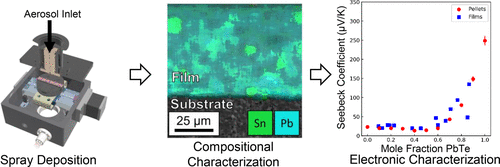
The discovery of new thermoelectric materials has the potential to benefit from advances in high-throughput methodologies. Traditional synthesis and characterization routes for thermoelectrics are time-consuming serial processes. In contrast, high-throughput materials discovery is commonly done by thin film growth, which may produce microstructures that are metastable or compositionally graded and, therefore, are challenging to characterize. As a middle ground between bulk synthesis and thin film deposition, we find that the aerosol deposition process can rapidly produce samples that exhibit electronic property trends consistent with those produced by traditional bulk means. We demonstrate rapid growth of discrete thermoelectric thick films of varying chemical compositions (Pb1-xSnxTe) from PbTe and SnTe polydisperse micrometer sized powder feedstocks. The high deposition rate (near 1 μm min-1) and resultant microstructures are advantageous as the diffusion length scales promote rapid thermal treatment and equilibrium phase formation. Room-temperature high-throughput measurements of the Seebeck coefficient and resistivity are compared to traditionally produced bulk materials. The Seebeck coefficient of the films follows the trends of traditional samples, but the resistivity is found to be more sensitive to microstructural effects. Ultimately, we demonstrate a framework for exploratory materials science using aerosol deposition and high-throughput characterization instrumentation.
中文翻译:

通过气溶胶沉积形成的合金化热电PbTe-SnTe膜。
新的热电材料的发现可能会受益于高通量方法学的进步。用于热电的传统合成和表征路线是耗时的串行过程。相反,高通量材料的发现通常是通过薄膜生长来完成的,薄膜生长可能会产生亚稳态或成分分级的微观结构,因此难以表征。作为本体合成和薄膜沉积之间的中间地基,我们发现气溶胶沉积过程可以快速生产出显示出与传统本体方式所产生的电子特性趋势一致的样品。我们证明了从PbTe和SnTe多分散微米级粉末原料中,不同化学成分(Pb1-xSnxTe)的离散热电厚膜的快速生长。高的沉积速率(接近1μmmin-1)和所得的微结构是有利的,因为扩散长度尺度促进了快速热处理和平衡相的形成。将塞贝克系数和电阻率的室温高通量测量结果与传统生产的散装材料进行了比较。薄膜的塞贝克系数遵循传统样品的趋势,但发现电阻率对微结构效应更敏感。最终,我们演示了使用气溶胶沉积和高通量表征仪器进行探索性材料科学的框架。高的沉积速率(接近1μmmin-1)和所得的微结构是有利的,因为扩散长度尺度促进了快速热处理和平衡相的形成。将塞贝克系数和电阻率的室温高通量测量结果与传统生产的散装材料进行了比较。薄膜的塞贝克系数遵循传统样品的趋势,但发现电阻率对微结构效应更敏感。最终,我们演示了使用气溶胶沉积和高通量表征仪器进行探索性材料科学的框架。高的沉积速率(接近1μmmin-1)和所得的微结构是有利的,因为扩散长度尺度促进了快速热处理和平衡相的形成。将塞贝克系数和电阻率的室温高通量测量结果与传统生产的散装材料进行了比较。薄膜的塞贝克系数遵循传统样品的趋势,但发现电阻率对微结构效应更敏感。最终,我们演示了使用气溶胶沉积和高通量表征仪器进行探索性材料科学的框架。将塞贝克系数和电阻率的室温高通量测量结果与传统生产的散装材料进行了比较。薄膜的塞贝克系数遵循传统样品的趋势,但发现电阻率对微结构效应更敏感。最终,我们演示了使用气溶胶沉积和高通量表征仪器进行探索性材料科学的框架。将塞贝克系数和电阻率的室温高通量测量结果与传统生产的散装材料进行了比较。薄膜的塞贝克系数遵循传统样品的趋势,但发现电阻率对微结构效应更敏感。最终,我们演示了使用气溶胶沉积和高通量表征仪器进行探索性材料科学的框架。
更新日期:2019-10-28
中文翻译:
通过气溶胶沉积形成的合金化热电PbTe-SnTe膜。
新的热电材料的发现可能会受益于高通量方法学的进步。用于热电的传统合成和表征路线是耗时的串行过程。相反,高通量材料的发现通常是通过薄膜生长来完成的,薄膜生长可能会产生亚稳态或成分分级的微观结构,因此难以表征。作为本体合成和薄膜沉积之间的中间地基,我们发现气溶胶沉积过程可以快速生产出显示出与传统本体方式所产生的电子特性趋势一致的样品。我们证明了从PbTe和SnTe多分散微米级粉末原料中,不同化学成分(Pb1-xSnxTe)的离散热电厚膜的快速生长。高的沉积速率(接近1μmmin-1)和所得的微结构是有利的,因为扩散长度尺度促进了快速热处理和平衡相的形成。将塞贝克系数和电阻率的室温高通量测量结果与传统生产的散装材料进行了比较。薄膜的塞贝克系数遵循传统样品的趋势,但发现电阻率对微结构效应更敏感。最终,我们演示了使用气溶胶沉积和高通量表征仪器进行探索性材料科学的框架。高的沉积速率(接近1μmmin-1)和所得的微结构是有利的,因为扩散长度尺度促进了快速热处理和平衡相的形成。将塞贝克系数和电阻率的室温高通量测量结果与传统生产的散装材料进行了比较。薄膜的塞贝克系数遵循传统样品的趋势,但发现电阻率对微结构效应更敏感。最终,我们演示了使用气溶胶沉积和高通量表征仪器进行探索性材料科学的框架。高的沉积速率(接近1μmmin-1)和所得的微结构是有利的,因为扩散长度尺度促进了快速热处理和平衡相的形成。将塞贝克系数和电阻率的室温高通量测量结果与传统生产的散装材料进行了比较。薄膜的塞贝克系数遵循传统样品的趋势,但发现电阻率对微结构效应更敏感。最终,我们演示了使用气溶胶沉积和高通量表征仪器进行探索性材料科学的框架。将塞贝克系数和电阻率的室温高通量测量结果与传统生产的散装材料进行了比较。薄膜的塞贝克系数遵循传统样品的趋势,但发现电阻率对微结构效应更敏感。最终,我们演示了使用气溶胶沉积和高通量表征仪器进行探索性材料科学的框架。将塞贝克系数和电阻率的室温高通量测量结果与传统生产的散装材料进行了比较。薄膜的塞贝克系数遵循传统样品的趋势,但发现电阻率对微结构效应更敏感。最终,我们演示了使用气溶胶沉积和高通量表征仪器进行探索性材料科学的框架。


 京公网安备 11010802027423号