npj 2D Materials and Applications ( IF 9.7 ) Pub Date : 2019-10-25 , DOI: 10.1038/s41699-019-0123-5 János Pető , Gergely Dobrik , Gergő Kukucska , Péter Vancsó , Antal A. Koós , János Koltai , Péter Nemes-Incze , Chanyong Hwang , Levente Tapasztó
|
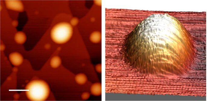
MoS2 single layers are valued for their sizeable direct bandgap at the heart of the envisaged electronic and optoelectronic applications. Here we experimentally demonstrate that moderate strain values (~2%) can already trigger an indirect bandgap transition and induce a finite charge carrier density in 2D MoS2 layers. A conclusive proof of the direct-to-indirect bandgap transition is provided by directly comparing the electronic and optical bandgaps of strained MoS2 single layers obtained from tunneling spectroscopy and photoluminescence measurements of MoS2 nanobubbles. Upon 2% biaxial tensile strain, the electronic gap becomes significantly smaller (1.45 ± 0.15 eV) than the optical direct gap (1.73 ± 0.1 eV), clearly evidencing a strain-induced direct to indirect bandgap transition. Moreover, the Fermi level can shift inside the conduction band already in moderately strained (~2%) MoS2 single layers conferring them a metallic character.
中文翻译:
MoS 2单层中的应变引起的间接带隙和传导电子
MoS 2单层以其可观的直接带隙而受到重视,这是设想的电子和光电应用的核心。在这里,我们通过实验证明,适度的应变值(〜2%)已经可以触发间接的带隙跃迁,并在2D MoS 2层中引起有限的载流子密度。通过直接比较由隧道光谱法和MoS 2的光致发光测量获得的应变MoS 2单层的电子和光学带隙,可以提供直接到间接带隙跃迁的结论性证据。纳米气泡。在2%的双轴拉伸应变下,电子间隙变得比光学直接间隙(1.73±0.1 eV)小得多(1.45±0.15 eV),清楚地证明了应变引起的直接带隙到间接带隙跃迁。此外,费米能级可以在已经处于中等应变(〜2%)的MoS 2单层中的导带内移动,从而赋予它们金属特性。


 京公网安备 11010802027423号