当前位置:
X-MOL 学术
›
Adv. Electron. Mater.
›
论文详情
Our official English website, www.x-mol.net, welcomes your
feedback! (Note: you will need to create a separate account there.)
Copper‐Leaf‐Based Process for Imperceptible Computational Electronics
Advanced Electronic Materials ( IF 5.3 ) Pub Date : 2019-10-25 , DOI: 10.1002/aelm.201900787 Séverine Mulatier 1, 2 , David Coulon 2 , Roger Delattre 1 , Sylvain Blayac 1 , Marc Ramuz 1
Advanced Electronic Materials ( IF 5.3 ) Pub Date : 2019-10-25 , DOI: 10.1002/aelm.201900787 Séverine Mulatier 1, 2 , David Coulon 2 , Roger Delattre 1 , Sylvain Blayac 1 , Marc Ramuz 1
Affiliation
|
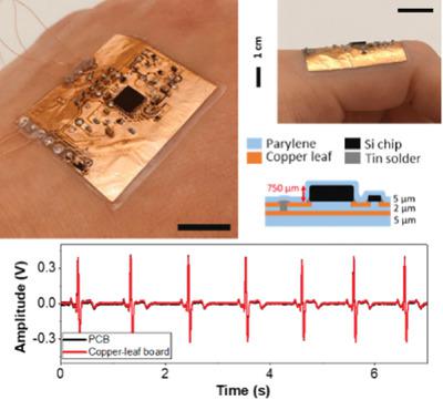
Imperceptible electronics have a key role in tomorrow's wearable technologies. Individual elements such as ultra‐thin sensors, batteries, solar cells, and actuators are well described in literature, but there is a lack of methods to build the computing circuit itself. A new process is presented for the fabrication of flexible and imperceptible circuits that reach standards of microelectronics associated with significant integration density of components and interconnections, as well as multilayering. The stack uses a commercialized decorative copper leaf with a thickness of 450 nm as the conductive layer and a parylene substrate of a few micrometers. The copper leaf shows both high compliance and conductivity of bulk copper (5.96 × 10⁷ S m−1), with electrical resistance stable over 5000 cycles of complete folding. The process requires stencil‐free laser patterning that reaches fine‐pitch integration, conventional soldering methods, and a three‐step via fabrication and assembly process for multilayered circuits. The functionality of an ultra‐thin, multilayered, lightweight, electrocardiogram‐monitoring device is demonstrated. This allows for direct transfer of microelectronic designs for rapid prototyping from rigid board to imperceptible electronics.
中文翻译:

不可感知的计算电子的铜叶基工艺
不易察觉的电子产品在明天的可穿戴技术中起着关键作用。文献中对超薄传感器,电池,太阳能电池和执行器等单个元素进行了很好的描述,但是缺少构建计算电路本身的方法。提出了一种新的制造柔性和不易察觉的电路的方法,该电路达到了微电子学的标准,与组件和互连以及多层的显着集成密度有关。堆叠使用厚度为450 nm的商品化装饰铜叶作为导电层和几微米的聚对二甲苯衬底。铜叶显示出高的顺从性和散装铜的导电性(5.96×10 7 S m -1),在完整折叠的5000次循环中电阻保持稳定。该过程需要无模板的激光图案化,该图案化可实现细间距集成,传统的焊接方法以及多层电路的三步通孔制造和组装过程。演示了超薄,多层,轻便的心电图监测设备的功能。这允许将微电子设计直接转移,以便从刚性板到不易察觉的电子产品快速进行原型制作。
更新日期:2020-01-13
中文翻译:
不可感知的计算电子的铜叶基工艺
不易察觉的电子产品在明天的可穿戴技术中起着关键作用。文献中对超薄传感器,电池,太阳能电池和执行器等单个元素进行了很好的描述,但是缺少构建计算电路本身的方法。提出了一种新的制造柔性和不易察觉的电路的方法,该电路达到了微电子学的标准,与组件和互连以及多层的显着集成密度有关。堆叠使用厚度为450 nm的商品化装饰铜叶作为导电层和几微米的聚对二甲苯衬底。铜叶显示出高的顺从性和散装铜的导电性(5.96×10 7 S m -1),在完整折叠的5000次循环中电阻保持稳定。该过程需要无模板的激光图案化,该图案化可实现细间距集成,传统的焊接方法以及多层电路的三步通孔制造和组装过程。演示了超薄,多层,轻便的心电图监测设备的功能。这允许将微电子设计直接转移,以便从刚性板到不易察觉的电子产品快速进行原型制作。


 京公网安备 11010802027423号