Light: Science & Applications ( IF 20.6 ) Pub Date : 2019-10-09 , DOI: 10.1038/s41377-019-0202-6 Yingtao Hu , Di Liang , Kunal Mukherjee , Youli Li , Chong Zhang , Geza Kurczveil , Xue Huang , Raymond G. Beausoleil
|
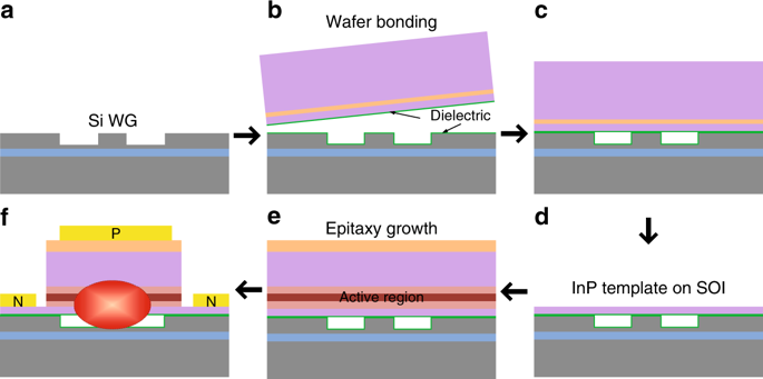
Silicon photonics is becoming a mainstream data-transmission solution for next-generation data centers, high-performance computers, and many emerging applications. The inefficiency of light emission in silicon still requires the integration of a III/V laser chip or optical gain materials onto a silicon substrate. A number of integration approaches, including flip-chip bonding, molecule or polymer wafer bonding, and monolithic III/V epitaxy, have been extensively explored in the past decade. Here, we demonstrate a novel photonic integration method of epitaxial regrowth of III/V on a III/V-on-SOI bonding template to realize heterogeneous lasers on silicon. This method decouples the correlated root causes, i.e., lattice, thermal, and domain mismatches, which are all responsible for a large number of detrimental dislocations in the heteroepitaxy process. The grown multi-quantum well vertical p–i–n diode laser structure shows a significantly low dislocation density of 9.5 × 104 cm−2, two orders of magnitude lower than the state-of-the-art conventional monolithic growth on Si. This low dislocation density would eliminate defect-induced laser lifetime concerns for practical applications. The fabricated lasers show room-temperature pulsed and continuous-wave lasing at 1.31 μm, with a minimal threshold current density of 813 A/cm2. This generic concept can be applied to other material systems to provide higher integration density, more functionalities and lower total cost for photonics as well as microelectronics, MEMS, and many other applications.
中文翻译:
通过使用新型光子集成方法在键合模板上再生III / V-on-Si MQW激光器
硅光子学正成为下一代数据中心,高性能计算机和许多新兴应用程序的主流数据传输解决方案。硅中发光效率低下仍然需要将III / V激光芯片或光学增益材料集成到硅基板上。在过去的十年中,已经广泛探索了许多集成方法,包括倒装芯片键合,分子或聚合物晶圆键合以及单片III / V外延。在这里,我们展示了一种新的光子集成方法,该方法在III / V-on-SOI键合模板上实现III / V的外延再生长,从而在硅上实现异质激光器。这种方法解耦了相关的根本原因,即晶格,热和域失配,它们都是造成异质外延过程中大量有害位错的原因。生长的多量子阱垂直p–i–n二极管激光器结构显示出极低的位错密度,为9.5×104 cm -2,比硅上最先进的传统单片生长低两个数量级。这种低位错密度将消除实际应用中由缺陷引起的激光寿命问题。制成的激光器显示出1.31μm的室温脉冲和连续波激光,最小阈值电流密度为813 A / cm 2。该通用概念可以应用于其他材料系统,以为光子学以及微电子学,MEMS和许多其他应用提供更高的集成密度,更多的功能和更低的总成本。


 京公网安备 11010802027423号