Nature Electronics ( IF 33.7 ) Pub Date : 2019-10-07 , DOI: 10.1038/s41928-019-0309-z Mirko Holler , Michal Odstrcil , Manuel Guizar-Sicairos , Maxime Lebugle , Elisabeth Müller , Simone Finizio , Gemma Tinti , Christian David , Joshua Zusman , Walter Unglaub , Oliver Bunk , Jörg Raabe , A. F. J. Levi , Gabriel Aeppli
|
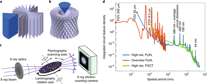
The imaging of integrated circuits across different length scales is required for failure analysis, design validation and quality control. At present, such inspection is accomplished using a hierarchy of different probes, from optical microscopy on the millimetre length scale to electron microscopy on the nanometre scale. Here we show that ptychographic X-ray laminography can provide non-destructive, three-dimensional views of integrated circuits, yielding both images of an entire chip volume and high-resolution images of arbitrarily chosen subregions. We demonstrate the approach using chips produced with 16 nm fin field-effect transistor technology, achieving a reconstruction resolution of 18.9 nm, and compare our results with photolithographic mask layout files and more conventional imaging approaches such as scanning electron microscopy. The technique should also be applicable to other branches of science and engineering where three-dimensional X-ray images of planar samples are required.
中文翻译:
宏观到纳米缩放的集成电路三维成像
对于故障分析,设计验证和质量控制,需要跨不同长度尺度的集成电路成像。目前,这种检查是使用不同探针的层次来完成的,从毫米级的光学显微镜到纳米级的电子显微镜。在这里,我们显示了谱图X射线层照相术可以提供集成电路的非破坏性三维视图,既可以显示整个芯片体积的图像,也可以生成任意选择的子区域的高分辨率图像。我们演示了使用16 nm鳍式场效应晶体管技术生产的芯片的方法,实现了18.9 nm的重建分辨率,并将我们的结果与光刻掩模版图文件和更常规的成像方法(如扫描电子显微镜)进行了比较。


 京公网安备 11010802027423号