当前位置:
X-MOL 学术
›
Nanoscale Horiz.
›
论文详情
Our official English website, www.x-mol.net, welcomes your
feedback! (Note: you will need to create a separate account there.)
Polarity-controllable MoS2 transistor for adjustable complementary logic inverter applications†
Nanoscale Horizons ( IF 8.0 ) Pub Date : 2019-08-23 , DOI: 10.1039/c9nh00275h Che-Yu Lin, Kristan Bryan Simbulan, Chuan-Jie Hong, Kai-Shin Li, Yuan-Liang Zhong, Yan-Kuin Su, Yann-Wen Lan
Nanoscale Horizons ( IF 8.0 ) Pub Date : 2019-08-23 , DOI: 10.1039/c9nh00275h Che-Yu Lin, Kristan Bryan Simbulan, Chuan-Jie Hong, Kai-Shin Li, Yuan-Liang Zhong, Yan-Kuin Su, Yann-Wen Lan
|
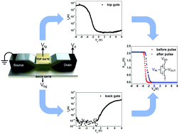
In this work, we introduce a MoS2-based field effect transistor that can alternately operate either as a p-type or an n-type semiconductor in the same device. The proposed device is built with an adjustable threshold voltage (Vth), which can be varied by adding a layer of plasma-oxidized dielectric at the top gate structure. This facilitates a surplus of oxygen due to the relatively thin grown dielectric layer and the creation of negative charges in that layer instead of the usual ones of positive polarization in the bottom dielectric layer. Consequently, the Vth shifts and the top gate structure switches from the typical n-type to p-type while the n-type behaviour remains in the application of the bottom-gate voltages. The Vth can be tuned further by applying a gate pulse input at the top gate. Accordingly, we have demonstrated complementary logic inverters with adjustable device characteristics that are controllable by the polarity of charges induced in the device's oxide layer. This is a big step towards the concurrent implementation of both n-type and p-type characteristics in a single device.
中文翻译:

用于可调互补逻辑逆变器应用的 极性可控MoS 2晶体管†
在这项工作中,我们介绍了基于MoS 2的场效应晶体管,该晶体管可以在同一设备中交替用作p型或n型半导体。所提出的器件具有可调节的阈值电压(V th),可以通过在顶栅结构上添加一层等离子体氧化的电介质来改变该阈值电压。由于相对较薄的生长的介电层和在该层中产生负电荷而不是底部介电层中通常的正极性电荷,这促进了氧气的过剩。因此,V th移位并且顶栅结构从典型的n型转变为p型,而在底栅电压的施加中n型行为仍然存在。这V th可以通过在顶栅极上施加栅极脉冲输入来进一步调整。因此,我们展示了具有可调节器件特性的互补逻辑反相器,该器件可通过器件氧化物层中感应出的电荷的极性来控制。这是朝着在单个器件中同时实现n型和p型特性迈出的一大步。
更新日期:2019-12-17
中文翻译:
用于可调互补逻辑逆变器应用的 极性可控MoS 2晶体管†
在这项工作中,我们介绍了基于MoS 2的场效应晶体管,该晶体管可以在同一设备中交替用作p型或n型半导体。所提出的器件具有可调节的阈值电压(V th),可以通过在顶栅结构上添加一层等离子体氧化的电介质来改变该阈值电压。由于相对较薄的生长的介电层和在该层中产生负电荷而不是底部介电层中通常的正极性电荷,这促进了氧气的过剩。因此,V th移位并且顶栅结构从典型的n型转变为p型,而在底栅电压的施加中n型行为仍然存在。这V th可以通过在顶栅极上施加栅极脉冲输入来进一步调整。因此,我们展示了具有可调节器件特性的互补逻辑反相器,该器件可通过器件氧化物层中感应出的电荷的极性来控制。这是朝着在单个器件中同时实现n型和p型特性迈出的一大步。


 京公网安备 11010802027423号