npj 2D Materials and Applications ( IF 9.1 ) Pub Date : 2019-06-13 , DOI: 10.1038/s41699-019-0106-6 Qingkai Qian , Jiacheng Lei , Jin Wei , Zhaofu Zhang , Gaofei Tang , Kailun Zhong , Zheyang Zheng , Kevin J. Chen
|
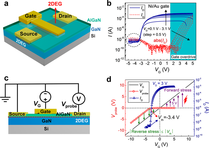
Various 2D/3D heterostructures can be created by harnessing the advantages of both the layered two-dimensional semiconductors and bulk materials. A semiconducting gate field-effect transistor (SG-FET) structure based on 2D/3D heterostructures is proposed here. The SG-FET is demonstrated on an AlGaN/GaN high-electron mobility transistor (HEMT) by adopting single-layer MoS2 as the gate electrode. The MoS2 semiconducting gate can effectively turn on and turn off the HEMT without sacrificing the subthreshold swing and breakdown voltage. Most importantly, the proposed semiconducting gate can deliver inherent over-voltage protection for field-effect transistors (FETs). Furthermore, the self-adjustable semiconducting gate potential with drain bias can even boost the ON-current while guaranteeing the safe operation of FET. In implementing the semiconducting gate, the layered two-dimensional materials such as the adopted MoS2 have several important benefits such as the feasibility of high-quality crystals on different gate dielectrics and the good controllability of semiconducting gate depletion threshold voltage by the layer thickness. The demonstrated semiconducting gate as over-voltage protection for HEMT can be extended to other FETs, which can become another advantageous arena for the possible applications of the layered two-dimensional materials.
中文翻译:
2D材料用作场效应晶体管的半导体栅极,具有固有的过压保护和增加的导通电流
利用分层二维半导体和块状材料的优点,可以创建各种2D / 3D异质结构。本文提出了一种基于2D / 3D异质结构的半导体栅场效应晶体管(SG-FET)结构。通过采用单层MoS 2作为栅电极,在AlGaN / GaN高电子迁移率晶体管(HEMT)上演示了SG-FET 。MoS 2半导体栅极可以有效地打开和关闭HEMT,而不会牺牲亚阈值摆幅和击穿电压。最重要的是,建议的半导体栅极可以为场效应晶体管(FET)提供固有的过压保护。此外,具有漏极偏置的自调节半导体栅极电势甚至可以提高导通电流,同时保证FET的安全运行。在实施半导体栅极时,需要采用分层的二维材料,例如采用的MoS 2具有几个重要的好处,例如在不同的栅极电介质上使用高质量晶体的可行性以及通过层厚度对半导体栅极耗尽阈值电压的良好可控性。作为HEMT的过电压保护,已证明的半导体栅极可以扩展到其他FET,对于分层二维材料的可能应用,这可以成为另一个有利的舞台。


 京公网安备 11010802027423号