Microsystems & Nanoengineering ( IF 7.3 ) Pub Date : 2019-05-06 , DOI: 10.1038/s41378-019-0056-3 Chaowei Wang 1 , Liang Yang 1 , Chenchu Zhang 2 , Shenglong Rao 1 , Yulong Wang 1 , Sizhu Wu 3 , Jiawen Li 1 , Yanlei Hu 1 , Dong Wu 1 , Jiaru Chu 1 , Koji Sugioka 4
|
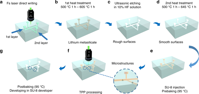
Multilayered microfluidic channels integrated with functional microcomponents are the general trend of future biochips, which is similar to the history of Si-integrated circuits from the planer to the three-dimensional (3D) configuration, since they offer miniaturization while increasing the integration degree and diversifying the applications in the reaction, catalysis, and cell cultures. In this paper, an optimized hybrid processing technology is proposed to create true multilayered microchips, by which “all-in-one” 3D microchips can be fabricated with a successive procedure of 3D glass micromachining by femtosecond-laser-assisted wet etching (FLAE) and the integration of microcomponents into the fabricated microchannels by two-photon polymerization (TPP). To create the multilayered microchannels at different depths in glass substrates (the top layer was embedded at 200 μm below the surface, and the underlying layers were constructed with a 200-μm spacing) with high uniformity and quality, the laser power density (13~16.9 TW/cm2) was optimized to fabricate different layers. To simultaneously complete the etching of each layer, which is also important to ensure the high uniformity, the control layers (nonlaser exposed regions) were prepared at the upper ends of the longitudinal channels. Solvents with different dyes were used to verify that each layer was isolated from the others. The high-quality integration was ensured by quantitatively investigating the experimental conditions in TPP, including the prebaking time (18~40 h), laser power density (2.52~3.36 TW/cm2) and developing time (0.8~4 h), all of which were optimized for each channel formed at different depths. Finally, the eight-layered microfluidic channels integrated with polymer microstructures were successfully fabricated to demonstrate the unique capability of this hybrid technique.
中文翻译:
通过混合“一体式”飞秒激光加工制造的多层摩天大楼微芯片
与功能微元件集成的多层微流体通道是未来生物芯片的大趋势,这类似于硅集成电路从平面到三维(3D)配置的历史,因为它们在提供小型化的同时提高集成度和多样化在反应、催化和细胞培养中的应用。在本文中,提出了一种优化的混合处理技术来创建真正的多层微芯片,通过该技术“可以通过飞秒激光辅助湿法蚀刻 (FLAE) 以及通过双光子聚合 (TPP) 将微组件集成到制造的微通道中的连续 3D 玻璃微加工程序来制造一体式 3D 微芯片。为了在玻璃基板中创建不同深度的多层微通道(顶层嵌入表面以下 200 μm,底层以 200 μm 间距构建)具有高均匀性和质量,激光功率密度(13~ 16.9 TW/cm 2) 被优化以制造不同的层。为了同时完成每一层的蚀刻,这对于确保高均匀性也很重要,在纵向通道的上端制备了控制层(非激光暴露区域)。使用具有不同染料的溶剂来验证每一层是否与其他层分离。通过定量研究 TPP 中的实验条件,包括预烘烤时间(18~40 h)、激光功率密度(2.52~3.36 TW/cm 2) 和发展时间 (0.8~4 h),所有这些都针对不同深度形成的每个通道进行了优化。最后,成功制造了与聚合物微结构集成的八层微流体通道,以证明这种混合技术的独特能力。


 京公网安备 11010802027423号