npj 2D Materials and Applications ( IF 9.1 ) Pub Date : 2019-04-29 , DOI: 10.1038/s41699-019-0101-y Paolo Paletti , Ruoyu Yue , Christopher Hinkle , Susan K. Fullerton-Shirey , Alan Seabaugh
|
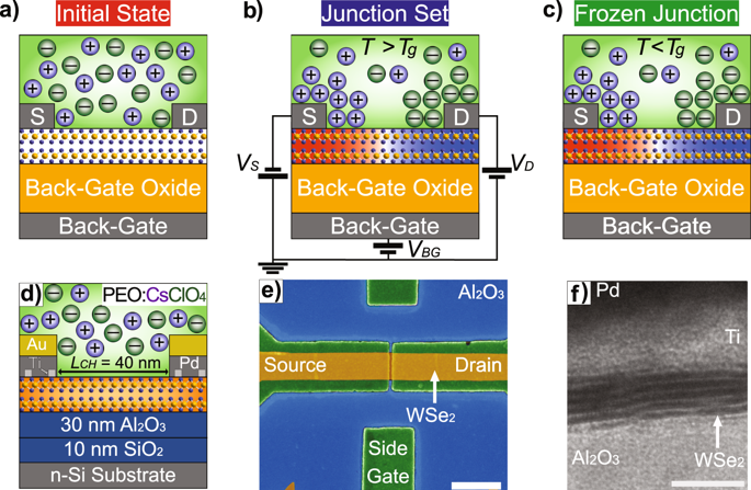
Two-dimensional van der Waals materials offer unique advantages for the development of band-to-band tunneling devices given their lack of dangling bonds, atomically flat thickness and steep band edges. Here, we present the experimental demonstration of an electric double layer (EDL) Esaki junction in synthetic WSe2 thin films. A Si-compatible process is developed for the fabrication of nanoscale FETs utilizing molecular beam epitaxy of WSe2 performed directly on top of a high-κ dielectric at back-end-of-line-friendly temperatures (<550 °C). Degenerate and abrupt doping profiles are obtained by modulating the electron/cation and hole/anion EDLs formed at the interface between a tens-of-nanometer long WSe2 channel and a solid polymer electrolyte, polyethylene oxide:cesium perchlorate (PEO:CsClO4). Numerical simulations are used to determine the bias dependence of the equilibrium ion and carrier density profiles. The EDL-doped tunnel diode exhibits repeatable, gate-tunable band-to-band tunneling with negative differential resistance in the forward bias regime at temperatures up to 140 K, and strong conduction in reverse bias. A maximum peak-to-valley current ratio of 3.5 is measured at 110 K.
中文翻译:
二维电双层Esaki二极管
由于二维范德华材料缺乏悬空键,原子厚度平坦且带边缘陡峭,因此它们为带间隧穿器件的开发提供了独特的优势。在这里,我们介绍合成WSe 2薄膜中的电双层(EDL)Esaki结的实验演示。开发了一种Si兼容工艺来制造纳米级FET,该工艺利用WSe 2的分子束外延技术直接在高κ介电层的后端友好温度(<550°C)上进行。通过调制在数十纳米长的WSe 2之间的界面上形成的电子/阳离子和空穴/阴离子EDL,可以获得简并的突变分布图。通道和固体聚合物电解质,聚环氧乙烷:高氯酸铯(PEO:CsClO 4)。数值模拟用于确定平衡离子和载流子密度曲线的偏差依赖性。掺杂EDL的隧道二极管表现出可重复的,栅极可调的带间隧穿,在温度高达140 K的正向偏置条件下具有负差分电阻,并且在反向偏置下具有强传导性。在110 K下测得的最大峰谷电流比为3.5。


 京公网安备 11010802027423号