npj 2D Materials and Applications ( IF 9.1 ) Pub Date : 2019-03-29 , DOI: 10.1038/s41699-019-0096-4 Juan Francisco Gonzalez Marin , Dmitrii Unuchek , Kenji Watanabe , Takashi Taniguchi , Andras Kis
|
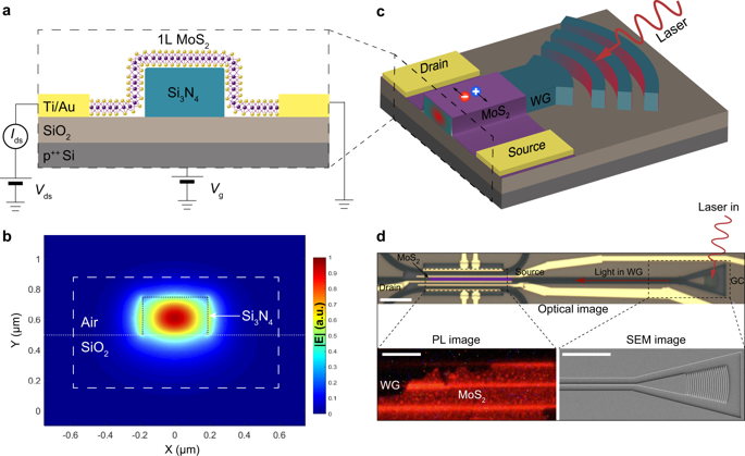
In recent years, two-dimensional materials have risen as an attractive platform for integrated optoelectronics, due to their atomic scale thickness, favorable electrical, mechanical, and optical properties. In particular, graphene has been exploited as an ultrafast light modulator and photodetector, operating at telecommunication wavelengths. However, materials with larger bandgaps are required for light detection in the visible range of the spectrum, with wide applications in space communication, industrial quality controls, light sensing, etc. Even though TMDC-based light emitting and detecting devices in the visible spectrum have already been realized, efficient light absorption and photocurrent generation on integrated devices has not been achieved yet. Here, we demonstrate the integration of an ultrasensitive MoS2 photodetector with a silicon nitride photonic circuit. In contrast to the limited vertical light absorption, we observe near-unity lateral absorption, which results in even higher responsivity. By fabricating an alternative device where the MoS2 semiconducting channel is combined with a hexagonal boron nitride (h-BN) substrate, we significantly improve the speed of the photodetector. Low power operation is further achieved in a third device with graphene local gates. These results pave the way for future TMDC-based integrated optoelectronic devices.
中文翻译:
集成了光子电路的MoS 2光电探测器
近年来,由于二维材料的原子尺度厚度,良好的电,机械和光学特性,二维材料已成为集成光电的有吸引力的平台。特别地,石墨烯已被用作在电信波长下工作的超快光调制器和光电检测器。但是,在光谱的可见范围内进行光检测需要具有较大带隙的材料,在空间通信,工业质量控制,光感测等方面具有广泛的应用。即使在可见光谱中基于TMDC的发光和检测设备具有已经认识到,尚未实现集成器件上的有效光吸收和光电流产生。在这里,我们演示了超灵敏MoS 2的集成带有氮化硅光子电路的光电探测器。与有限的垂直光吸收相反,我们观察到近统一的横向吸收,这导致了更高的响应度。通过制造将MoS 2半导体通道与六方氮化硼(h-BN)基板组合在一起的替代设备,我们可以显着提高光电探测器的速度。在具有石墨烯局部栅极的第三器件中进一步实现了低功率操作。这些结果为未来基于TMDC的集成光电设备铺平了道路。


 京公网安备 11010802027423号