npj 2D Materials and Applications ( IF 9.1 ) Pub Date : 2019-03-14 , DOI: 10.1038/s41699-019-0095-5 Michael G. Stanford , Yu-Chuan Lin , Maria Gabriela Sales , Anna N. Hoffman , Christopher T. Nelson , Kai Xiao , Stephen McDonnell , Philip D. Rack
|
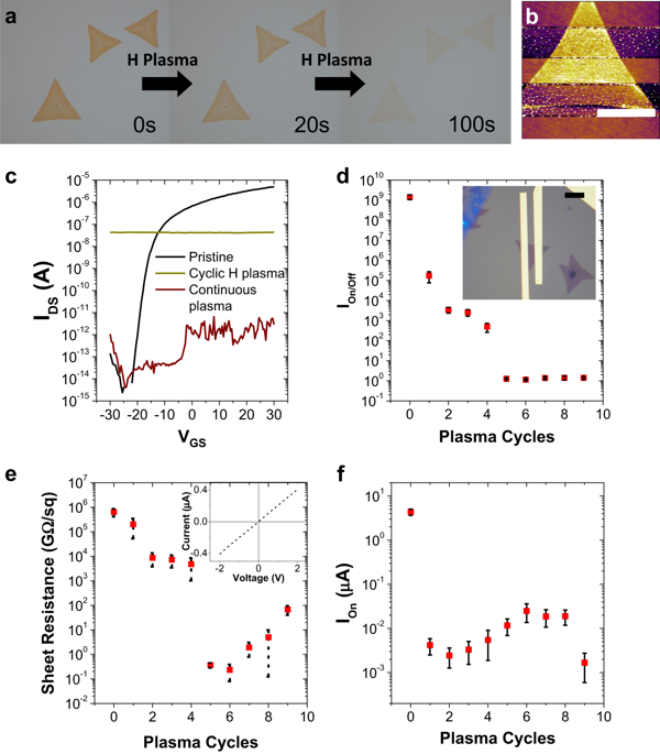
Tailoring the electrical transport properties of two-dimensional transition metal dichalcogenides can enable the formation of atomically thin circuits. In this work, cyclic hydrogen and oxygen plasma exposures are utilized to introduce defects and oxidize MoS2 in a controlled manner. This results in the formation of sub-stochiometric MoO3−x, which transforms the semiconducting behavior to metallic conduction. To demonstrate functionality, single flakes of MoS2 were lithographically oxidized using electron beam lithography and subsequent plasma exposures. This enabled the formation of atomically thin inverters from a single flake of MoS2, which represents an advancement toward atomically thin circuitry.
中文翻译:
通过等离子处理在单层MoS 2中进行光刻图案化的金属导电
调整二维过渡金属二卤化物的电传输性质可以实现原子上薄的电路的形成。在这项工作中,利用循环氢和氧等离子体暴露来引入缺陷并以受控方式氧化MoS 2。这导致形成亚化学计量的MoO 3 - x,将半导体行为转变为金属导电。为了证明功能,使用电子束光刻和随后的等离子体曝光对单片MoS 2进行光刻氧化。这使得能够从单片MoS 2薄片形成原子薄的逆变器,这代表了朝原子薄电路的发展。


 京公网安备 11010802027423号