当前位置:
X-MOL 学术
›
Adv. Mater.
›
论文详情
Our official English website, www.x-mol.net, welcomes your feedback! (Note: you will need to create a separate account there.)
Area-Selective Chemical Vapor Deposition of Gold by Electron Beam Seeding
Advanced Materials ( IF 29.4 ) Pub Date : 2024-03-28 , DOI: 10.1002/adma.202313571 Aleksei Tsarapkin 1 , Krzysztof Maćkosz 2 , Chinmai Sai Jureddy 2 , Ivo Utke 2 , Katja Höflich 1
Advanced Materials ( IF 29.4 ) Pub Date : 2024-03-28 , DOI: 10.1002/adma.202313571 Aleksei Tsarapkin 1 , Krzysztof Maćkosz 2 , Chinmai Sai Jureddy 2 , Ivo Utke 2 , Katja Höflich 1
Affiliation
|
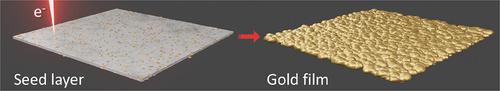
Chemical vapor deposition (CVD) is an established method for producing high-purity thin films, but it typically necessitates the pre- and post-processing using a mask to produce structures. This study presents a novel maskless patterning technique that enables area-selective CVD of gold. A focused electron beam is used to decompose the metal–organic precursor Au(acac)Me2 locally, thereby creating an autocatalytically active seed layer for subsequent CVD with the same precursor. The procedure can be included in the same CVD process without the need for clean room lithographic processing. Moreover, it operates at low temperatures of 80 °C, over 200 K lower than standard CVD temperatures for this precursor, reducing thermal load on the specimen. Given that electron beam seeding operates on any even moderately conductive surface, the process does not constrain device design. This is demonstrated by the example of vertical nanostructures with high aspect ratios of ≈40:1 and more. Written using a focused electron beam and the same precursor, these nanopillars exhibit catalytically active nuclei on their surface. Furthermore, by using the onset of the autocatalytic CVD growth, for the first time the local temperature increase caused by the writing of nanostructures with an electron beam can be precisely determined.
中文翻译:

通过电子束播种进行金的区域选择性化学气相沉积
化学气相沉积 (CVD) 是一种生产高纯度薄膜的成熟方法,但通常需要使用掩模进行预处理和后处理来生产结构。这项研究提出了一种新型无掩模图案化技术,可实现金的区域选择性 CVD。聚焦电子束用于局部分解金属有机前体 Au(acac)Me 2,从而为后续使用相同前体的 CVD 创建自催化活性种子层。该过程可以包含在同一 CVD 工艺中,无需洁净室光刻处理。此外,它在 80 °C 的低温下运行,比该前驱体的标准 CVD 温度低 200 K 以上,从而减少了样品上的热负荷。鉴于电子束播种可以在任何中等导电表面上进行,因此该过程不会限制设备设计。具有约 40:1 及以上高纵横比的垂直纳米结构的示例证明了这一点。这些纳米柱使用聚焦电子束和相同的前驱体编写,在其表面表现出催化活性核。此外,通过利用自催化CVD生长的开始,首次可以精确地确定由电子束写入纳米结构引起的局部温度升高。
更新日期:2024-03-28
中文翻译:
通过电子束播种进行金的区域选择性化学气相沉积
化学气相沉积 (CVD) 是一种生产高纯度薄膜的成熟方法,但通常需要使用掩模进行预处理和后处理来生产结构。这项研究提出了一种新型无掩模图案化技术,可实现金的区域选择性 CVD。聚焦电子束用于局部分解金属有机前体 Au(acac)Me 2,从而为后续使用相同前体的 CVD 创建自催化活性种子层。该过程可以包含在同一 CVD 工艺中,无需洁净室光刻处理。此外,它在 80 °C 的低温下运行,比该前驱体的标准 CVD 温度低 200 K 以上,从而减少了样品上的热负荷。鉴于电子束播种可以在任何中等导电表面上进行,因此该过程不会限制设备设计。具有约 40:1 及以上高纵横比的垂直纳米结构的示例证明了这一点。这些纳米柱使用聚焦电子束和相同的前驱体编写,在其表面表现出催化活性核。此外,通过利用自催化CVD生长的开始,首次可以精确地确定由电子束写入纳米结构引起的局部温度升高。


 京公网安备 11010802027423号