当前位置:
X-MOL 学术
›
Org. Electron.
›
论文详情
Our official English website, www.x-mol.net, welcomes your feedback! (Note: you will need to create a separate account there.)
Power-efficient and high-performance potential of pentacene transistors enabled by metal-nitride gate insulators fabricated with nitrogen plasma
Organic Electronics ( IF 3.2 ) Pub Date : 2024-03-18 , DOI: 10.1016/j.orgel.2024.107034 Yu Wu Wang , Pravinraj Selvaraj , Yu Han Cheng , Zheng Han Chen , Ming Han Chi
Organic Electronics ( IF 3.2 ) Pub Date : 2024-03-18 , DOI: 10.1016/j.orgel.2024.107034 Yu Wu Wang , Pravinraj Selvaraj , Yu Han Cheng , Zheng Han Chen , Ming Han Chi
|
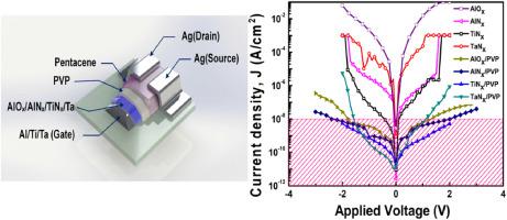
The demand for next-generation organic field-effect transistors (OFETs) with low operating voltage is becoming gradually attractive in many application areas, such as flexible/wearable medical sensors and stretchable electronics. While using high dielectric materials is a potent approach, it often results in a decline in field-effect mobility or on/off ratio. Unfortunately, achieving low-voltage operation has hindered practical applications, compromising device performance. Here, we discovered for the first time a novel class of low-driving voltage pentacene transistors adopting gate insulators composed of nitrogen-plasma-reacted AlN, TiN, and TaN. This exciting discovery is simple, affordable, environmentally friendly, and secure. X-ray photoelectron spectrometer (XPS) analysis reveals that the as-formed metal nitrides are composited with certain native oxide components, exhibiting outstanding leakage current blocking capacity and a high dielectric constant. Further, the surface energy of metal nitrides was altered by applying a thin layer of poly-(4-vinylphenol) (PVP). This modification improved the growth of pentacene grains and the insulator/pentacene interface. The best devices by comprehensive evaluation, the TiN samples, achieve a high average of field-effect mobility ∼1.41 cm/Vs, a subthreshold swing of 0.19 V/dec, an on/off current ratio of ∼10, and a turn-on voltage close to 0 V, which shows promising potential candidates for the flexible electronic devices, optoelectronic devices, and neuromorphic application.
中文翻译:

利用氮等离子体制造的金属氮化物栅极绝缘体实现并五苯晶体管的高能效和高性能潜力
在许多应用领域,例如柔性/可穿戴医疗传感器和可拉伸电子产品,对具有低工作电压的下一代有机场效应晶体管(OFET)的需求逐渐变得有吸引力。虽然使用高介电材料是一种有效的方法,但它通常会导致场效应迁移率或开/关比下降。不幸的是,实现低电压工作阻碍了实际应用,损害了器件性能。在这里,我们首次发现了一类新型低驱动电压并五苯晶体管,采用由氮等离子体反应的 AlN、TiN 和 TaN 组成的栅极绝缘体。这一令人兴奋的发现简单、经济、环保且安全。 X射线光电子能谱(XPS)分析表明,所形成的金属氮化物与某些天然氧化物成分复合,表现出出色的漏电流阻挡能力和高介电常数。此外,通过施加一薄层聚(4-乙烯基苯酚)(PVP)来改变金属氮化物的表面能。这种修饰改善了并五苯晶粒和绝缘体/并五苯界面的生长。经过综合评估,最好的器件 TiN 样品实现了高平均场效应迁移率 ~1.41 cm/Vs、亚阈值摆幅为 0.19 V/dec、开/关电流比为 ~10,以及开启电压接近 0 V,这显示了柔性电子器件、光电器件和神经形态应用的有希望的潜在候选者。
更新日期:2024-03-18
中文翻译:
利用氮等离子体制造的金属氮化物栅极绝缘体实现并五苯晶体管的高能效和高性能潜力
在许多应用领域,例如柔性/可穿戴医疗传感器和可拉伸电子产品,对具有低工作电压的下一代有机场效应晶体管(OFET)的需求逐渐变得有吸引力。虽然使用高介电材料是一种有效的方法,但它通常会导致场效应迁移率或开/关比下降。不幸的是,实现低电压工作阻碍了实际应用,损害了器件性能。在这里,我们首次发现了一类新型低驱动电压并五苯晶体管,采用由氮等离子体反应的 AlN、TiN 和 TaN 组成的栅极绝缘体。这一令人兴奋的发现简单、经济、环保且安全。 X射线光电子能谱(XPS)分析表明,所形成的金属氮化物与某些天然氧化物成分复合,表现出出色的漏电流阻挡能力和高介电常数。此外,通过施加一薄层聚(4-乙烯基苯酚)(PVP)来改变金属氮化物的表面能。这种修饰改善了并五苯晶粒和绝缘体/并五苯界面的生长。经过综合评估,最好的器件 TiN 样品实现了高平均场效应迁移率 ~1.41 cm/Vs、亚阈值摆幅为 0.19 V/dec、开/关电流比为 ~10,以及开启电压接近 0 V,这显示了柔性电子器件、光电器件和神经形态应用的有希望的潜在候选者。


 京公网安备 11010802027423号