当前位置:
X-MOL 学术
›
ACS Appl. Mater. Interfaces
›
论文详情
Our official English website, www.x-mol.net, welcomes your
feedback! (Note: you will need to create a separate account there.)
Corona Poling Induced Phase Transition to Highly Polar Phase in P(VDF-TrFE-CFE) Dielectric and Charge Transport of Organic Field-Effect Transistors
ACS Applied Materials & Interfaces ( IF 8.3 ) Pub Date : 2023-06-01 , DOI: 10.1021/acsami.3c04435 Yina Moon 1 , Yeon-Ju Kim 1, 2 , Dongseong Yang 1 , Nara Han 1 , Minwoo Lee 1 , Dong-Yu Kim 1
ACS Applied Materials & Interfaces ( IF 8.3 ) Pub Date : 2023-06-01 , DOI: 10.1021/acsami.3c04435 Yina Moon 1 , Yeon-Ju Kim 1, 2 , Dongseong Yang 1 , Nara Han 1 , Minwoo Lee 1 , Dong-Yu Kim 1
Affiliation
|
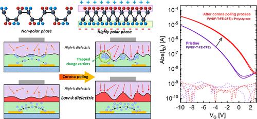
Increasing the number of charge carriers flowing through the charge transport channel to improve the electrical performance of organic field-effect transistors (OFETs) is important because it leads to a low driving voltage and a high drain current value. This paper proposes a new strategy, the corona poling process, to enhance the electrical performance of OFETs using an external electric field when forming a dielectric film using a PVDF-based high-k dielectric terpolymer, P(VDF-TrFE-CFE). A corona poling process was applied to align the dipoles with high-k dielectric molecules and improve the capacitance, thereby increasing the number of charge carriers. Through this process, by observing the phase transition of a PVDF dielectric through a corona poling process in the GIWAXS data, the phase transition through an external electric field was thoroughly revealed for the first time. As a result, the capacitance of high-k dielectric films can be improved, and the amount of charge carriers can be increased by a simple corona poling process. In addition, to reduce the effect of deep trap sites caused by the dipole alignment, a thin low-k dielectric, polystyrene (PS), was introduced between the active and high-k dielectric layers to provide trap site passivation, thereby increasing the electrical performance of the OFET. Therefore, through this strategy, using a diketopyrrolopyrrole (DPP)-based donor–acceptor (D–A) copolymer as an active material of OFET, the average saturation region hole mobility was improved from 0.34 to 0.60 cm2/Vs. Thus, the electrical performances of the OFETs were improved by enhancing the capacitance through the corona poling process and reducing the charge carrier trap sites introduced by the high-k and low-k bi-layer dielectric layer. Importantly, this work offers a new strategy for the post-treatment to improve electrical performance of organic devices.
中文翻译:

电晕极化诱导 P(VDF-TrFE-CFE) 电介质中向高极性相的相变以及有机场效应晶体管的电荷传输
增加流过电荷传输通道的电荷载流子数量对于提高有机场效应晶体管 (OFET) 的电性能非常重要,因为这会导致低驱动电压和高漏极电流值。本文提出了一种新策略,即电晕极化工艺,在使用基于 PVDF 的高 k 介电三元聚合物 P(VDF-TrFE-CFE) 形成介电薄膜时,利用外部电场来增强 OFET 的电性能。采用电晕极化工艺使偶极子与高 k 介电分子对齐并提高电容,从而增加电荷载流子的数量。通过这个过程,通过 GIWAXS 数据中的电晕极化过程观察 PVDF 电介质的相变,首次彻底揭示了通过外部电场的相变。结果,可以提高高k介电膜的电容,并且可以通过简单的电晕极化工艺增加载流子的量。此外,为了减少偶极子排列引起的深陷阱位点的影响,在有源层和高k电介质层之间引入薄的低k电介质聚苯乙烯(PS),以提供陷阱位点钝化,从而提高电学性能。 OFET 的性能。因此,通过该策略,使用基于二酮吡咯并吡咯(DPP)的供体-受体(D-A)共聚物作为OFET的活性材料,平均饱和区空穴迁移率从0.34 cm-1提高到0.60 cm-1 通过简单的电晕极化工艺可以提高高k介电薄膜的电容,并且可以增加载流子的数量。此外,为了减少偶极子排列引起的深陷阱位点的影响,在有源层和高k电介质层之间引入薄的低k电介质聚苯乙烯(PS),以提供陷阱位点钝化,从而提高电学性能。 OFET 的性能。因此,通过该策略,使用基于二酮吡咯并吡咯(DPP)的供体-受体(D-A)共聚物作为OFET的活性材料,平均饱和区空穴迁移率从0.34 cm-1提高到0.60 cm-1 通过简单的电晕极化工艺可以提高高k介电薄膜的电容,并且可以增加载流子的数量。此外,为了减少偶极子排列引起的深陷阱位点的影响,在有源层和高k电介质层之间引入薄的低k电介质聚苯乙烯(PS),以提供陷阱位点钝化,从而提高电学性能。 OFET 的性能。因此,通过该策略,使用基于二酮吡咯并吡咯(DPP)的供体-受体(D-A)共聚物作为OFET的活性材料,平均饱和区空穴迁移率从0.34 cm-1提高到0.60 cm-1 在有源层和高 k 介电层之间引入聚苯乙烯 (PS),以提供陷阱位点钝化,从而提高 OFET 的电性能。因此,通过该策略,使用基于二酮吡咯并吡咯(DPP)的供体-受体(D-A)共聚物作为OFET的活性材料,平均饱和区空穴迁移率从0.34 cm-1提高到0.60 cm-1 在有源层和高 k 介电层之间引入聚苯乙烯 (PS),以提供陷阱位点钝化,从而提高 OFET 的电性能。因此,通过该策略,使用基于二酮吡咯并吡咯(DPP)的供体-受体(D-A)共聚物作为OFET的活性材料,平均饱和区空穴迁移率从0.34 cm-1提高到0.60 cm-12 /Vs。因此,通过电晕极化过程增强电容并减少高k和低k双层介电层引入的电荷载流子陷阱位点,OFET的电性能得到改善。重要的是,这项工作为后处理提高有机器件的电性能提供了一种新策略。
更新日期:2023-06-01
中文翻译:
电晕极化诱导 P(VDF-TrFE-CFE) 电介质中向高极性相的相变以及有机场效应晶体管的电荷传输
增加流过电荷传输通道的电荷载流子数量对于提高有机场效应晶体管 (OFET) 的电性能非常重要,因为这会导致低驱动电压和高漏极电流值。本文提出了一种新策略,即电晕极化工艺,在使用基于 PVDF 的高 k 介电三元聚合物 P(VDF-TrFE-CFE) 形成介电薄膜时,利用外部电场来增强 OFET 的电性能。采用电晕极化工艺使偶极子与高 k 介电分子对齐并提高电容,从而增加电荷载流子的数量。通过这个过程,通过 GIWAXS 数据中的电晕极化过程观察 PVDF 电介质的相变,首次彻底揭示了通过外部电场的相变。结果,可以提高高k介电膜的电容,并且可以通过简单的电晕极化工艺增加载流子的量。此外,为了减少偶极子排列引起的深陷阱位点的影响,在有源层和高k电介质层之间引入薄的低k电介质聚苯乙烯(PS),以提供陷阱位点钝化,从而提高电学性能。 OFET 的性能。因此,通过该策略,使用基于二酮吡咯并吡咯(DPP)的供体-受体(D-A)共聚物作为OFET的活性材料,平均饱和区空穴迁移率从0.34 cm-1提高到0.60 cm-1 通过简单的电晕极化工艺可以提高高k介电薄膜的电容,并且可以增加载流子的数量。此外,为了减少偶极子排列引起的深陷阱位点的影响,在有源层和高k电介质层之间引入薄的低k电介质聚苯乙烯(PS),以提供陷阱位点钝化,从而提高电学性能。 OFET 的性能。因此,通过该策略,使用基于二酮吡咯并吡咯(DPP)的供体-受体(D-A)共聚物作为OFET的活性材料,平均饱和区空穴迁移率从0.34 cm-1提高到0.60 cm-1 通过简单的电晕极化工艺可以提高高k介电薄膜的电容,并且可以增加载流子的数量。此外,为了减少偶极子排列引起的深陷阱位点的影响,在有源层和高k电介质层之间引入薄的低k电介质聚苯乙烯(PS),以提供陷阱位点钝化,从而提高电学性能。 OFET 的性能。因此,通过该策略,使用基于二酮吡咯并吡咯(DPP)的供体-受体(D-A)共聚物作为OFET的活性材料,平均饱和区空穴迁移率从0.34 cm-1提高到0.60 cm-1 在有源层和高 k 介电层之间引入聚苯乙烯 (PS),以提供陷阱位点钝化,从而提高 OFET 的电性能。因此,通过该策略,使用基于二酮吡咯并吡咯(DPP)的供体-受体(D-A)共聚物作为OFET的活性材料,平均饱和区空穴迁移率从0.34 cm-1提高到0.60 cm-1 在有源层和高 k 介电层之间引入聚苯乙烯 (PS),以提供陷阱位点钝化,从而提高 OFET 的电性能。因此,通过该策略,使用基于二酮吡咯并吡咯(DPP)的供体-受体(D-A)共聚物作为OFET的活性材料,平均饱和区空穴迁移率从0.34 cm-1提高到0.60 cm-12 /Vs。因此,通过电晕极化过程增强电容并减少高k和低k双层介电层引入的电荷载流子陷阱位点,OFET的电性能得到改善。重要的是,这项工作为后处理提高有机器件的电性能提供了一种新策略。


 京公网安备 11010802027423号