Applied Surface Science ( IF 6.3 ) Pub Date : 2023-05-30 , DOI: 10.1016/j.apsusc.2023.157613 Hong Li , Yuhang Liu , Shuai Sun , Fengbin Liu , Jing Lu
|
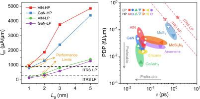
The shrinking of transistors to ultra-scale limits is in great demand to extend Moore’s law, where the search for proper alternative channel materials is significant. The III-V group compounds are regarded as post-Si candidates for their high electron mobility. Herein, we simulate the monolayer (ML) AlN and GaN metal-oxide-semiconductor field-effect transistors (MOSFETs) with ab initio quantum transport simulation to evaluate their device performance limit. The ML AlN and GaN MOSFETs exhibit much better n-type performances than their p-type counterparts, and the n-type ML AlN (GaN) MOSFETs can surpass the International Roadmap for Device and Systems (IRDS, 2022 version) lower-power (LP) and high-performance (HP) target for the year 2028 even at gate length (Lg) of 3 and 2 nm, respectively. Encouragingly, the optimal n-type ML AlN (GaN) MOSFETs possess the highest (second-highest) Ion against all studied n-type ML MOSFETs and propel the Lg limit that outperforms the International Technology Roadmap for Semiconductors (ITRS, 2013 version) LP and HP targets to 2 and 1 (2) nm, respectively.
中文翻译:
单层 AlN 和 GaN MOSFET 的缩放限制
非常需要将晶体管缩小到超规模极限以扩展摩尔定律,其中寻找合适的替代通道材料非常重要。III-V族化合物因其高电子迁移率而被视为后硅候选物。在此,我们使用从头算量子传输模拟来模拟单层 (ML) AlN 和 GaN 金属氧化物半导体场效应晶体管 (MOSFET),以评估它们的器件性能极限。ML AlN 和 GaN MOSFET 表现出比其p型同类产品更好的n型性能,并且n型 ML AlN (GaN) MOSFET 即使在栅极长度 ( L g )分别为 3 和 2 纳米。令人鼓舞的是,最佳n型 ML AlN (GaN) MOSFET 拥有最高(第二高)的I on与所有研究的n型 ML MOSFET 相比,推动L g限制超过国际半导体技术路线图(ITRS,2013 版) ) LP 和 HP 目标分别为 2 和 1 (2) nm。


 京公网安备 11010802027423号