当前位置:
X-MOL 学术
›
Adv. Mater.
›
论文详情
Our official English website, www.x-mol.net, welcomes your
feedback! (Note: you will need to create a separate account there.)
Near Zero-Threshold Voltage P-N Junction Diodes Based on Super-Semiconducting Nanostructured Ag/Al Arrays
Advanced Materials ( IF 27.4 ) Pub Date : 2023-02-01 , DOI: 10.1002/adma.202210612 Zhigang Li 1 , Jiteng Li 1 , Weike Wang 2 , Qijie Yan 2 , Yongrui Zhou 1 , Luping Zhu 3 , Bingqiang Cao 3 , Bingqing Wei 4
Advanced Materials ( IF 27.4 ) Pub Date : 2023-02-01 , DOI: 10.1002/adma.202210612 Zhigang Li 1 , Jiteng Li 1 , Weike Wang 2 , Qijie Yan 2 , Yongrui Zhou 1 , Luping Zhu 3 , Bingqiang Cao 3 , Bingqing Wei 4
Affiliation
|
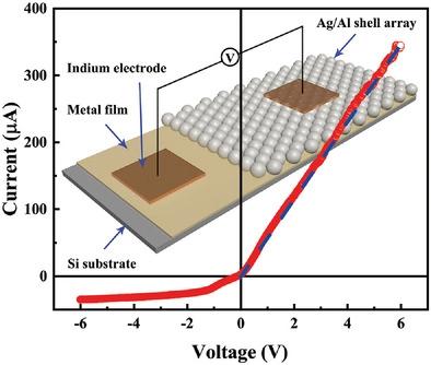
Semiconductor devices are currently one of the most common energy consumption devices. Significantly reducing the energy consumption of semiconductor devices with advanced energy-efficient technologies is highly desirable. The discovery of super-semiconductors (SSCs) based on metallic bi-layer shell arrays provides an opportunity to realize ultra-low-power consumption semiconductor devices. As an example, the achievement of near zero-threshold voltage in p-n junction diodes based on super-semiconducting nanostructured Ag/Al arrays is reported, realizing ultra-low-power p-n junction diodes: ≈3 W per trillion diodes with a working voltage of 1 V or 30 mW per trillion diodes with an operating voltage of 0.1 V. In addition, the p-n junction diodes exhibit a high breakdown field of ≈1.1 × 10⁶ V cm−1, similar to that of SiC and GaN, due to a robust built-in field driven by infrared light photons. The SSC p-n diodes with near zero-threshold voltage and high breakdown field allow access to ultra-low-power semiconducting transistors, integrated circuits, chips, etc.
中文翻译:

基于超半导体纳米结构 Ag/Al 阵列的近零阈值电压 PN 结二极管
半导体器件是目前最常见的耗能器件之一。非常需要采用先进的节能技术显着降低半导体器件的能耗。基于金属双层壳阵列的超半导体 (SSC) 的发现为实现超低功耗半导体器件提供了机会。例如,据报道,基于超半导体纳米结构 Ag/Al 阵列的 pn 结二极管实现了近零阈值电压,实现了超低功率 pn 结二极管:≈3 W/万亿二极管,工作电压为1 V 或 30 mW 每万亿二极管,工作电压为 0.1 V。此外,pn 结二极管具有 ≈1.1 × 10 6 V cm −1的高击穿场,类似于 SiC 和 GaN,这是由于由红外光光子驱动的强大内置场。具有接近零阈值电压和高击穿场的 SSC pn 二极管允许访问超低功率半导体晶体管、集成电路、芯片等。
更新日期:2023-02-01
中文翻译:
基于超半导体纳米结构 Ag/Al 阵列的近零阈值电压 PN 结二极管
半导体器件是目前最常见的耗能器件之一。非常需要采用先进的节能技术显着降低半导体器件的能耗。基于金属双层壳阵列的超半导体 (SSC) 的发现为实现超低功耗半导体器件提供了机会。例如,据报道,基于超半导体纳米结构 Ag/Al 阵列的 pn 结二极管实现了近零阈值电压,实现了超低功率 pn 结二极管:≈3 W/万亿二极管,工作电压为1 V 或 30 mW 每万亿二极管,工作电压为 0.1 V。此外,pn 结二极管具有 ≈1.1 × 10 6 V cm −1的高击穿场,类似于 SiC 和 GaN,这是由于由红外光光子驱动的强大内置场。具有接近零阈值电压和高击穿场的 SSC pn 二极管允许访问超低功率半导体晶体管、集成电路、芯片等。


 京公网安备 11010802027423号