当前位置:
X-MOL 学术
›
Chem. Mater.
›
论文详情
Our official English website, www.x-mol.net, welcomes your
feedback! (Note: you will need to create a separate account there.)
First-Principles Calculation Guided High-Purity Layer Control of 4 in. MoS2 by Plasma RIE
Chemistry of Materials ( IF 7.2 ) Pub Date : 2023-01-18 , DOI: 10.1021/acs.chemmater.2c02914 Changmin Kim 1, 2 , Muyoung Kim 1 , Donghyun Cho 1, 3 , Chaitanya Kaluram Kanade 4 , Hyunho Seok 4 , Moon Soo Bak 2 , Daewoong Kim 1 , Woo Seok Kang 1 , Taesung Kim 2, 4 , Hyeong-U Kim 1
Chemistry of Materials ( IF 7.2 ) Pub Date : 2023-01-18 , DOI: 10.1021/acs.chemmater.2c02914 Changmin Kim 1, 2 , Muyoung Kim 1 , Donghyun Cho 1, 3 , Chaitanya Kaluram Kanade 4 , Hyunho Seok 4 , Moon Soo Bak 2 , Daewoong Kim 1 , Woo Seok Kang 1 , Taesung Kim 2, 4 , Hyeong-U Kim 1
Affiliation
|
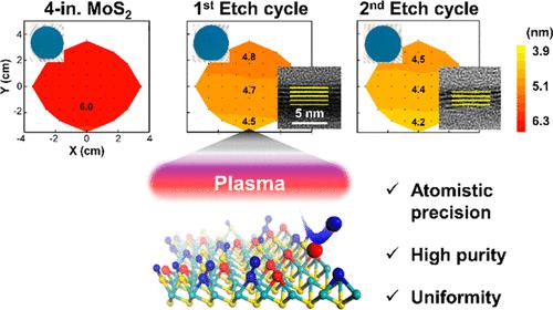
Two-dimensional molybdenum disulfide (MoS2) is one of the most promising candidates for next-generation semiconductors. Among the advantages offered by MoS2, a tunable bandgap that depends on the thickness is essential for the on-demand manufacturing of nanoelectronics. For this reason, elaborate layer control of MoS2 has been a long-standing research objective. However, prior efforts had several critical issues including surface roughness, poor uniformity/scalability, and impurities. Through this study, we aimed to achieve both ultrahigh precision and purity in large-scale (4 in.) layer control of MoS2 by two consecutive plasma processes: plasma-enhanced chemical vapor deposition (PECVD) and reactive ion etching (RIE). The 4 in. wafer-scale MoS2 was synthesized by PECVD, and the as-grown bulk layers were etched using RIE with a computationally screened gas mixture in the cyclic step. For every RIE cycle, the 4 in. MoS2 wafer was evenly etched to a thickness of 0.3–0.4 nm while there was no damage to the atomic structure and chemical impurities. For the computational screening of candidate gases, first-principles calculations explored the energetics of surface reaction and offered physical insights into the associated electronic interaction. The combination of computational screening and experimentation accelerates optimal process design and provides an in-depth understanding of the plasma–surface interactions.
中文翻译:

第一性原理计算指导的 4 in. MoS2 等离子 RIE 的高纯度层控制
二维二硫化钼 (MoS 2 ) 是下一代半导体最有前途的候选材料之一。在 MoS 2提供的优势中,取决于厚度的可调带隙对于纳米电子产品的按需制造至关重要。因此,MoS 2的精细层控制一直是一个长期的研究目标。然而,之前的努力存在几个关键问题,包括表面粗糙度、均匀性/可扩展性差和杂质。通过这项研究,我们的目标是在 MoS 2的大规模(4 英寸)层控制中实现超高精度和纯度通过两个连续的等离子体工艺:等离子体增强化学气相沉积 (PECVD) 和反应离子蚀刻 (RIE)。4 英寸晶圆级 MoS 2通过 PECVD 合成,并且在循环步骤中使用 RIE 和计算筛选的气体混合物蚀刻生长的体层。对于每个 RIE 循环,4 英寸的 MoS 2wafer被均匀蚀刻到0.3-0.4 nm的厚度,同时没有破坏原子结构和化学杂质。对于候选气体的计算筛选,第一性原理计算探索了表面反应的能量学,并提供了对相关电子相互作用的物理见解。计算筛选和实验的结合加速了优化工艺设计,并提供了对等离子体-表面相互作用的深入理解。
更新日期:2023-01-18
中文翻译:
第一性原理计算指导的 4 in. MoS2 等离子 RIE 的高纯度层控制
二维二硫化钼 (MoS 2 ) 是下一代半导体最有前途的候选材料之一。在 MoS 2提供的优势中,取决于厚度的可调带隙对于纳米电子产品的按需制造至关重要。因此,MoS 2的精细层控制一直是一个长期的研究目标。然而,之前的努力存在几个关键问题,包括表面粗糙度、均匀性/可扩展性差和杂质。通过这项研究,我们的目标是在 MoS 2的大规模(4 英寸)层控制中实现超高精度和纯度通过两个连续的等离子体工艺:等离子体增强化学气相沉积 (PECVD) 和反应离子蚀刻 (RIE)。4 英寸晶圆级 MoS 2通过 PECVD 合成,并且在循环步骤中使用 RIE 和计算筛选的气体混合物蚀刻生长的体层。对于每个 RIE 循环,4 英寸的 MoS 2wafer被均匀蚀刻到0.3-0.4 nm的厚度,同时没有破坏原子结构和化学杂质。对于候选气体的计算筛选,第一性原理计算探索了表面反应的能量学,并提供了对相关电子相互作用的物理见解。计算筛选和实验的结合加速了优化工艺设计,并提供了对等离子体-表面相互作用的深入理解。


 京公网安备 11010802027423号